10 AI Acceleration
Resources: Slides, Videos, Exercises, Labs
Deploying ML on edge devices presents challenges such as limited processing speed, memory constraints, and stringent energy efficiency requirements. To overcome these challenges, specialized hardware acceleration is key. Hardware accelerators are designed to optimize compute-intensive tasks like inference by using custom silicon chips tailored for matrix multiplications, providing significant speedups compared to general-purpose CPUs. This enables real-time execution of advanced models on devices with strict constraints on size, weight, and power.
Understand why hardware acceleration is needed for AI workloads
Survey key accelerator options like GPUs, TPUs, FPGAs, and ASICs and their tradeoffs
Learn about programming models, frameworks, and compilers for AI accelerators
Appreciate the importance of benchmarking and metrics for hardware evaluation
Recognize the role of hardware-software co-design in building efficient systems
Gain exposure to cutting-edge research directions like neuromorphic and quantum computing
Understand how ML is beginning to augment and improve hardware design
10.1 Introduction
You’ve probably noticed the growing demand for embedding machine learning into everyday devices—like the smartphones in our pockets, smart home appliances, and even autonomous vehicles. Bringing ML capabilities into these real-world environments is exciting, but it comes with its own set of challenges. Unlike powerful data center servers, these edge devices have limited computing resources, making it tricky to run complex models effectively.
Specialized hardware acceleration is the key to making high-performance machine learning possible on resource-limited edge devices. When we talk about hardware acceleration, we’re referring to the use of custom chips and architectures designed to handle the heavy lifting of ML operations, taking the burden off the main processor. In neural networks, some of the most demanding tasks involve matrix multiplications during inference. Hardware accelerators are built to optimize these operations, often delivering 10-100x speedups compared to general-purpose CPUs. This kind of acceleration is what makes it feasible to run advanced neural network models on devices that are constrained by size, weight, and power— and to do it all in real-time.
In this chapter, we’ll take a closer look at the different hardware acceleration techniques available for embedded machine learning and the tradeoffs that come with each option. The goal is to give you a solid understanding of how these techniques work, so you can make informed decisions when it comes to choosing the right hardware and optimizing your software. By the end, you’ll be well-equipped to develop high-performance machine learning capabilities on edge devices, even with their constraints.
10.2 Background and Basics
10.2.1 Historical Background
The origins of hardware acceleration date back to the 1960s, with the advent of floating point math co-processors to offload calculations from the main CPU. One early example was the Intel 8087 chip released in 1980 to accelerate floating point operations for the 8086 processor. This established the practice of using specialized processors to handle math-intensive workloads efficiently.
In the 1990s, the first graphics processing units (GPUs) emerged to process graphics pipelines for rendering and gaming rapidly. Nvidia’s GeForce 256 in 1999 was one of the earliest programmable GPUs capable of running custom software algorithms. GPUs exemplify domain-specific fixed-function accelerators and evolve into parallel programmable accelerators.
In the 2000s, GPUs were applied to general-purpose computing under GPGPU. Their high memory bandwidth and computational throughput made them well-suited for math-intensive workloads. This included breakthroughs in using GPUs to accelerate training of deep learning models such as AlexNet in 2012.
In recent years, Google’s Tensor Processing Units (TPUs) represent customized ASICs specifically architected for matrix multiplication in deep learning. During inference, their optimized tensor cores achieve higher TeraOPS/watt than CPUs or GPUs. Ongoing innovation includes model compression techniques like pruning and quantization to fit larger neural networks on edge devices.
This evolution demonstrates how hardware acceleration has focused on solving compute-intensive bottlenecks, from floating point math to graphics to matrix multiplication for ML. Understanding this history provides a crucial context for specialized AI accelerators today.
10.2.2 The Need for Acceleration
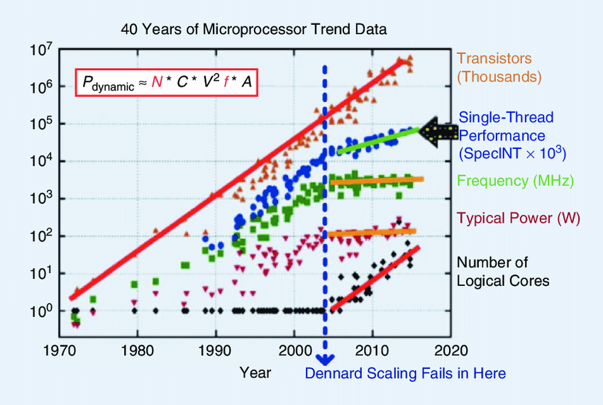
The evolution of hardware acceleration is closely tied to the broader history of computing. Central to this history is the role of transistors, the fundamental building blocks of modern electronics. Transistors act as tiny switches that can turn on or off, enabling the complex computations that drive everything from simple calculators to advanced machine learning models. In the early decades, chip design was governed by Moore’s Law, which predicted that the number of transistors on an integrated circuit would double approximately every two years, and Dennard Scaling, which observed that as transistors became smaller, their performance (speed) increased, while power density (power per unit area) remained constant. These two laws were held through the single-core era. Figure 10.1 shows the trends of different microprocessor metrics. As the figure denotes, Dennard Scaling fails around the mid-2000s; notice how the clock speed (frequency) remains almost constant even as the number of transistors keeps increasing.
However, as Patterson and Hennessy (2016) describes, technological constraints eventually forced a transition to the multicore era, with chips containing multiple processing cores to deliver performance gains. Power limitations prevented further scaling, which led to “dark silicon” (Dark Silicon), where not all chip areas could be simultaneously active (Xiu 2019).
“Dark silicon” refers to portions of the chip that cannot be powered simultaneously due to thermal and power limitations. Essentially, as the density of transistors increased, the proportion of the chip that could be actively used without overheating or exceeding power budgets shrank.
This phenomenon meant that while chips had more transistors, not all could be operational simultaneously, limiting potential performance gains. This power crisis necessitated a shift to the accelerator era, with specialized hardware units tailored for specific tasks to maximize efficiency. The explosion in AI workloads further drove demand for customized accelerators. Enabling factors included new programming languages, software tools, and manufacturing advances.
Fundamentally, hardware accelerators are evaluated on performance, power, and silicon area (PPA)—the nature of the target application—whether memory-bound or compute-bound—heavily influences the design. For example, memory-bound workloads demand high bandwidth and low latency access, while compute-bound applications require maximal computational throughput.
10.2.3 General Principles
The design of specialized hardware accelerators involves navigating complex tradeoffs between performance, power efficiency, silicon area, and workload-specific optimizations. This section outlines core considerations and methodologies for achieving an optimal balance based on application requirements and hardware constraints.
Performance Within Power Budgets
To understand how to achieve the right balance between performance and power budgets, it’s important to first define a few key concepts that play a crucial role in this process. Performance broadly refers to the overall capability of a system to complete computational tasks effectively within given constraints. One of the key components of performance is throughput, which is the rate at which these tasks are processed, commonly measured in floating point operations per second (FLOPS) or frames per second (FPS). Throughput depends heavily on parallelism—the ability of the hardware to carry out multiple operations simultaneously—and clock frequency, which is the speed at which the processor cycles through these operations. Higher throughput typically leads to better performance, but it also increases power consumption as activity rises.
Simply maximizing throughput is not enough; the efficiency of the hardware also matters. Efficiency is the measure of how many operations are performed per watt of power consumed, reflecting the relationship between computational work and energy use. In scenarios where power is a limiting factor, such as in edge devices, achieving high efficiency is critical. To help you remember how these concepts interconnect, consider the following relationships:
- Performance = Throughput * Efficiency
- Throughput ~= Parallelism * Clock Frequency
- Efficiency = Operations / Watt
Hardware accelerators aim to maximize performance within set power budgets. This requires careful balancing of parallelism, the chip’s clock frequency, the operating voltage, workload optimization, and other techniques to maximize operations per watt.
For example, GPUs achieve high throughput via massively parallel architectures. However, their efficiency is lower than that of customized application-specific integrated circuits (ASICs) like Google’s TPU, which optimize for a specific workload.
Managing Silicon Area and Costs
The size of a chip’s area has a direct impact on its manufacturing cost. To understand why, it helps to know a bit about the manufacturing process.
Chips are created from large, thin slices of semiconductor material known as wafers. During manufacturing, each wafer is divided into multiple smaller blocks called dies, with each die containing the circuitry for an individual chip. After the wafer is processed, it’s cut into these individual dies, which are then packaged to form the final chips used in electronic devices.
Larger dies require more material and are more prone to defects, which can lower the yield—meaning fewer usable chips are produced from each wafer. While manufacturers can scale designs by combining multiple smaller dies into a single package (multi-die packages), this adds complexity and cost to the packaging and production process.
The amount of silicon area needed on a die depends on several factors:
- Computational resources - e.g., number of cores, memory, caches
- Manufacturing process node - smaller transistors enable higher density
- Programming model - programmed accelerators require more flexibility
Accelerator design involves squeezing maximum performance within these silicon area constraints. Techniques like pruning and compression help fit larger models onto the chip without exceeding the available space.
Workload-Specific Optimizations
Designing effective hardware accelerators requires tailoring the architecture to the specific demands of the target workload. Different types of workloads—whether in AI, graphics, or robotics—have unique characteristics that dictate how the accelerator should be optimized.
Some of the key considerations when optimizing hardware for specific workloads include:
- Memory vs Compute boundedness: Memory-bound workloads require more memory bandwidth, while compute-bound apps need arithmetic throughput.
- Data locality: Data movement should be minimized for efficiency. Near-compute memory helps.
- Bit-level operations: Low precision datatypes like INT8/INT4 optimize compute density.
- Data parallelism: Multiple replicated compute units allow parallel execution.
- Pipelining: Overlapped execution of operations increases throughput.
Understanding workload characteristics enables customized acceleration. For example, convolutional neural networks use sliding window operations optimally mapped to spatial arrays of processing elements.
By understanding these architectural tradeoffs, designers can make informed decisions about the hardware accelerator’s architecture, ensuring that it delivers the best possible performance for its intended use.
Sustainable Hardware Design
In recent years, AI sustainability has become a pressing concern driven by two key factors - the exploding scale of AI workloads and their associated energy consumption.
First, the size of AI models and datasets has rapidly grown. For example, based on OpenAI’s AI computing trends, the amount of computing used to train state-of-the-art models doubles every 3.5 months. This exponential growth requires massive computational resources in data centers.
Second, the energy usage of AI training and inference presents sustainability challenges. Data centers running AI applications consume substantial energy, contributing to high carbon emissions. It’s estimated that training a large AI model can have a carbon footprint of 626,000 pounds of CO2 equivalent, almost 5 times the lifetime emissions of an average car.
To address these challenges, sustainable hardware design focuses on optimizing energy efficiency without compromising performance. This involves developing specialized accelerators that minimize energy consumption while maximizing computational throughput.
We will learn about Sustainable AI in a later chapter, where we will discuss it in more detail.
10.3 Accelerator Types
Hardware accelerators can take on many forms. They can exist as a widget (like the Neural Engine in the Apple M1 chip) or as entire chips specially designed to perform certain tasks very well. This section will examine processors for machine learning workloads along the spectrum from highly specialized ASICs to more general-purpose CPUs.
We first focus on custom hardware purpose-built for AI to understand the most extreme optimizations possible when design constraints are removed. This establishes a ceiling for performance and efficiency. We then progressively consider more programmable and adaptable architectures, discussing GPUs and FPGAs. These make tradeoffs in customization to maintain flexibility. Finally, we cover general-purpose CPUs that sacrifice optimizations for a particular workload in exchange for versatile programmability across applications.
By structuring the analysis along this spectrum, we aim to illustrate the fundamental tradeoffs between utilization, efficiency, programmability, and flexibility in accelerator design. The optimal balance point depends on the constraints and requirements of the target application. This spectrum perspective provides a framework for reasoning about hardware choices for machine learning and the capabilities required at each level of specialization.
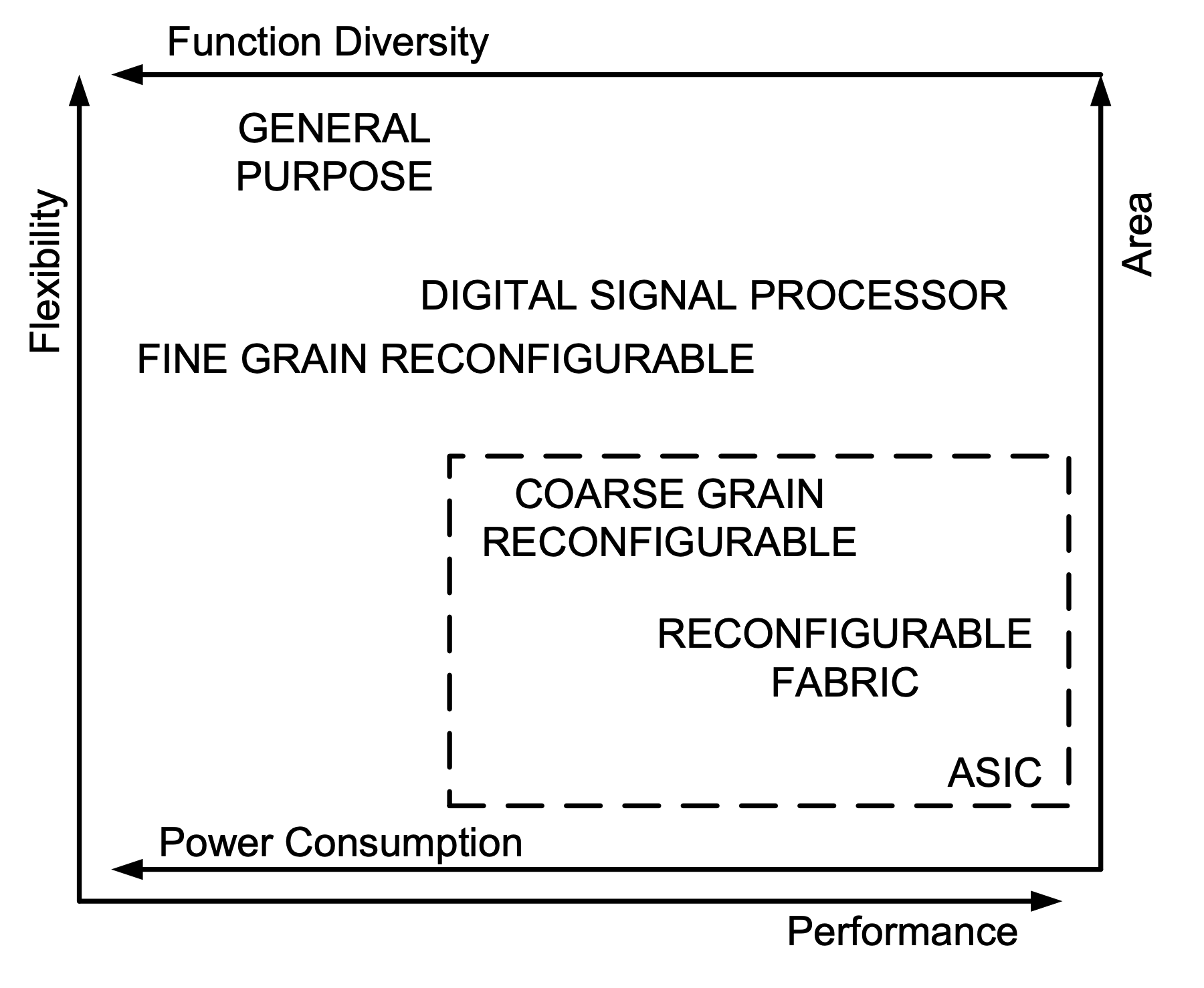
Figure 10.2 illustrates the complex interplay between flexibility, performance, functional diversity, and area of architecture design. Notice how the ASIC is on the bottom-right corner, with minimal area, flexibility, and power consumption and maximal performance, due to its highly specialized application-specific nature. A key tradeoff is functional diversity vs performance: general purpose architectures can serve diverse applications but their application performance is degraded as compared to more customized architectures.
The progression begins with the most specialized option, ASICs purpose-built for AI, to ground our understanding in the maximum possible optimizations before expanding to more generalizable architectures. This structured approach elucidates the accelerator design space.
10.3.1 Application-Specific Integrated Circuits (ASICs)
An Application-Specific Integrated Circuit (ASIC) is a type of integrated circuit (IC) that is custom-designed for a specific application or workload rather than for general-purpose use. Unlike CPUs and GPUs, ASICs do not support multiple applications or workloads. Rather, they are optimized to perform a single task extremely efficiently. The Google TPU is an example of an ASIC.
ASICs achieve this efficiency by tailoring every aspect of the chip design - the underlying logic gates, electronic components, architecture, memory, I/O, and manufacturing process - specifically for the target application. This level of customization allows removing any unnecessary logic or functionality required for general computation. The result is an IC that maximizes performance and power efficiency on the desired workload. The efficiency gains from application-specific hardware are so substantial that these software-centric firms dedicate enormous engineering resources to designing customized ASICs.
The rise of more complex machine learning algorithms has made the performance advantages enabled by tailored hardware acceleration a key competitive differentiator, even for companies traditionally concentrated on software engineering. ASICs have become a high-priority investment for major cloud providers aiming to offer faster AI computation.
Advantages
Due to their customized nature, ASICs provide significant benefits over general-purpose processors like CPUs and GPUs. The key advantages include the following.
Maximized Performance and Efficiency
The most fundamental advantage of ASICs is maximizing performance and power efficiency by customizing the hardware architecture specifically for the target application. Every transistor and design aspect is optimized for the desired workload - no unnecessary logic or overhead is needed to support generic computation.
For example, Google’s Tensor Processing Units (TPUs) contain architectures tailored exactly for the matrix multiplication operations used in neural networks. To design the TPU ASICs, Google’s engineering teams need to define the chip specifications clearly, write the architecture description using Hardware Description Languages like Verilog, synthesize the design to map it to hardware components, and carefully place-and-route transistors and wires based on the fabrication process design rules. This complex design process, known as very-large-scale integration (VLSI), allows them to build an optimized IC for machine learning workloads.
As a result, TPU ASICs achieve over an order of magnitude higher efficiency in operations per watt than general-purpose GPUs on ML workloads by maximizing performance and minimizing power consumption through a full-stack custom hardware design.
Specialized On-Chip Memory
ASICs incorporate on-chip memory, such as SRAM (Static Random Access Memory), and caches that are specifically optimized to feed data to the computational units. SRAM is a type of memory that is faster and more reliable than DRAM (Dynamic Random Access Memory) because it does not need to be periodically refreshed. However, it requires more transistors per bit of data, making it take up more space and more expensive to produce as compared to DRAM.
SRAM is ideal for on-chip memory, where speed is critical. The advantage of having large amounts of high-bandwidth, on-chip SRAM is that data can be stored close to the processing elements, allowing for rapid access. This provides tremendous speed advantages compared to acessing off-chip DRAM, which, although larger in capacity, can be up to 100x slower. For example, Apple’s M1 system-on-a-chip contains special low-latency SRAM to accelerate the performance of its Neural Engine machine learning hardware.
Data locality and optimizing memory hierarchy are crucial for high throughput and low power. Table 10.1 shows “Numbers Everyone Should Know,” from Jeff Dean.
| Operation | Latency |
|---|---|
| L1 cache reference | 0.5 ns |
| Branch mispredict | 5 ns |
| L2 cache reference | 7 ns |
| Mutex lock/unlock | 25 ns |
| Main memory reference | 100 ns |
| Compress 1K bytes with Zippy | 3,000 ns (3 us) |
| Send 1 KB bytes over 1 Gbps network | 10,000 ns (10 us) |
| Read 4 KB randomly from SSD | 150,000 ns (150 us) |
| Read 1 MB sequentially from memory | 250,000 ns (250 us) |
| Round trip within same datacenter | 500,000 ns (0.5 ms) |
| Read 1 MB sequentially from SSD | 1,000,000 ns (1 ms) |
| Disk seek | 10,000,000 ns (10 ms) |
| Read 1 MB sequentially from disk | 20,000,000 ns (20 ms) |
| Send packet CA → Netherlands → CA | 150,000,000 ns (150 ms) |
Custom Datatypes and Operations
Unlike general-purpose processors, ASICs can be designed to natively support custom datatypes like INT4 or bfloat16, which are widely used in ML models. For instance, Nvidia’s Ampere GPU architecture has dedicated bfloat16 Tensor Cores to accelerate AI workloads. Low-precision datatypes enable higher arithmetic density and performance. Please refer to Section 8.6 for additional details. ASICs can also directly incorporate non-standard operations common in ML algorithms as primitive operations - for example, natively supporting activation functions like ReLU makes execution more efficient.
High Parallelism
ASIC architectures can leverage higher parallelism tuned for the target workload versus general-purpose CPUs or GPUs. More computational units tailored for the application mean more operations execute simultaneously. Highly parallel ASICs achieve tremendous throughput for data parallel workloads like neural network inference.
Advanced Process Nodes
Cutting-edge manufacturing processes allow more transistors to be packed into smaller die areas, increasing density. ASICs designed specifically for high-volume applications can better amortize the costs of cutting-edge process nodes.
Disadvantages
Long Design Timelines
The engineering process of designing and validating an ASIC can take 2-3 years. Synthesizing the architecture using hardware description languages, taping out the chip layout, and fabricating the silicon on advanced process nodes involve long development cycles. For example, to tape out a 7nm chip, teams need to define specifications carefully, write the architecture in HDL, synthesize the logic gates, place components, route all interconnections, and finalize the layout to send for fabrication. This very large-scale integration (VLSI) flow means ASIC design and manufacturing can traditionally take 2-5 years.
There are a few key reasons why the long design timelines of ASICs, often 2-3 years, can be challenging for machine learning workloads:
- ML algorithms evolve rapidly: New model architectures, training techniques, and network optimizations are constantly emerging. For example, Transformers became hugely popular in NLP last few years. When an ASIC finishes tapeout, the optimal architecture for a workload may have changed.
- Datasets grow quickly: ASICs designed for certain model sizes or datatypes can become undersized relative to demand. For instance, natural language models are scaling exponentially with more data and parameters. A chip designed for BERT might not accommodate GPT-3.
- ML applications change frequently: The industry focus shifts between computer vision, speech, NLP, recommender systems, etc. An ASIC optimized for image classification may have less relevance in a few years.
- Faster design cycles with GPUs/FPGAs: Programmable accelerators like GPUs can adapt much quicker by upgrading software libraries and frameworks. New algorithms can be deployed without hardware changes.
- Time-to-market needs: Getting a competitive edge in ML requires rapidly experimenting with and deploying new ideas. Waiting several years for an ASIC is different from fast iteration.
The pace of innovation in ML needs to be better matched to the multi-year timescale for ASIC development. Significant engineering efforts are required to extend ASIC lifespan through modular architectures, process scaling, model compression, and other techniques. However, the rapid evolution of ML makes fixed-function hardware challenging.
High Non-Recurring Engineering Costs
The fixed costs of taking an ASIC from design to high-volume manufacturing can be very capital-intensive, often tens of millions of dollars. Photomask fabrication for taping out chips in advanced process nodes, packaging, and one-time engineering efforts is expensive. For instance, a 7nm chip tape-out alone could cost millions. The high non-recurring engineering (NRE) investment narrows ASIC viability to high-volume production use cases where the upfront cost can be amortized.
Complex Integration and Programming
ASICs require extensive software integration work, including drivers, compilers, OS support, and debugging tools. They also need expertise in electrical and thermal packaging. Additionally, efficiently programming ASIC architectures can involve challenges like workload partitioning and scheduling across many parallel units. The customized nature necessitates significant integration efforts to turn raw hardware into fully operational accelerators.
While ASICs provide massive efficiency gains on target applications by tailoring every aspect of the hardware design to one specific task, their fixed nature results in tradeoffs in flexibility and development costs compared to programmable accelerators, which must be weighed based on the application.
10.3.2 Field-Programmable Gate Arrays (FPGAs)
FPGAs are programmable integrated circuits that can be reconfigured for different applications. Their customizable nature provides advantages for accelerating AI algorithms compared to fixed ASICs or inflexible GPUs. While Google, Meta, and NVIDIA are considering putting ASICs in data centers, Microsoft deployed FPGAs in its data centers (Putnam et al. 2014) in 2011 to efficiently serve diverse data center workloads.
FPGAs have found widespread application in various fields, including medical imaging, robotics, and finance, where they excel in handling computationally intensive machine learning tasks. In medical imaging, an illustrative example is the application of FPGAs for brain tumor segmentation, a traditionally time-consuming and error-prone process. Compared to traditional GPU and CPU implementations, FPGAs have demonstrated over 5x and 44x performance improvements, respectively, and 11x and 82x gains in energy efficiency, highlighting their potential for demanding applications (Xiong et al. 2021).
Advantages
FPGAs provide several benefits over GPUs and ASICs for accelerating machine learning workloads.
Flexibility Through Reconfigurable Fabric
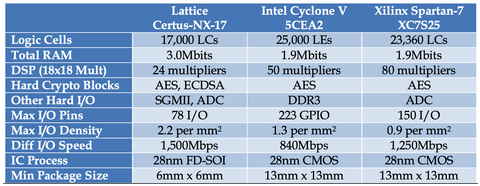
The key advantage of FPGAs is the ability to reconfigure the underlying fabric to implement custom architectures optimized for different models, unlike fixed-function ASICs. For example, quant trading firms use FPGAs to accelerate their algorithms because they change frequently, and the low NRE cost of FPGAs is more viable than tapping out new ASICs. Figure 10.3 contains a table comparing three different FPGAs.
FPGAs comprise basic building blocks - configurable logic blocks, RAM blocks, and interconnects. Vendors provide a base amount of these resources, and engineers program the chips by compiling HDL code into bitstreams that rearrange the fabric into different configurations. This makes FPGAs adaptable as algorithms evolve.
While FPGAs may not achieve the utmost performance and efficiency of workload-specific ASICs, their programmability provides more flexibility as algorithms change. This adaptability makes FPGAs a compelling choice for accelerating evolving machine learning applications.
Customized Parallelism and Pipelining
FPGA architectures can leverage spatial parallelism and pipelining by tailoring the hardware design to mirror the parallelism in ML models. For example, Intel’s HARPv2 FPGA platform splits the layers of an MNIST convolutional network across separate processing elements to maximize throughput. Unique parallel patterns like tree ensemble evaluations are also possible on FPGAs. Deep pipelines with optimized buffering and dataflow can be customized to each model’s structure and datatypes. This level of tailored parallelism and pipelining is not feasible on GPUs.
Low Latency On-Chip Memory
Large amounts of high-bandwidth on-chip memory enable localized storage for weights and activations. For instance, Xilinx Versal FPGAs contain 32MB of low-latency RAM blocks and dual-channel DDR4 interfaces for external memory. Bringing memory physically closer to the compute units reduces access latency. This provides significant speed advantages over GPUs that traverse PCIe or other system buses to reach off-chip GDDR6 memory.
Native Support for Low Precision
A key advantage of FPGAs is the ability to natively implement any bit width for arithmetic units, such as INT4 or bfloat16, used in quantized ML models. For example, Intel’s Stratix 10 NX FPGAs have dedicated INT8 cores that can achieve up to 143 INT8 TOPS (Tera Operations Per Second) at ~1 TOPS/W (Tera Operations Per Second per Watt) Intel Stratix 10 NX FPGA. TOPS is a measure of performance similar to FLOPS, but while FLOPS measures floating-point calculations, TOPS measures the number of integer operations a system can perform per second. Lower bit widths, like INT8 or INT4, increase arithmetic density and performance. FPGAs can even support mixed precision or dynamic precision tuning at runtime.
Disadvantages
Lower Peak Throughput than ASICs
FPGAs cannot match the raw throughput numbers of ASICs customized for a specific model and precision. The overheads of the reconfigurable fabric compared to fixed function hardware result in lower peak performance. For example, the TPU v5e pods allow up to 256 chips to be connected with more than 100 petaOps (Peta Operations Per Second) of INT8 performance, while FPGAs can offer up to 143 INT8 TOPS or 286 INT4 TOPS Intel Stratix 10 NX FPGA. PetaOps represents quadrillions of operations per second, whereas TOPS measures trillions, highlighting the much greater throughput capability of TPU pods compared to FPGAs.
This is because FPGAs comprise basic building blocks—configurable logic blocks, RAM blocks, and interconnects. Vendors provide a set amount of these resources. To program FPGAs, engineers write HDL code and compile it into bitstreams that rearrange the fabric, which has inherent overheads versus an ASIC purpose-built for one computation.
Programming Complexity
To optimize FPGA performance, engineers must program the architectures in low-level hardware description languages like Verilog or VHDL. This requires hardware design expertise and longer development cycles than higher-level software frameworks like TensorFlow. Maximizing utilization can be challenging despite advances in high-level synthesis from C/C++.
Reconfiguration Overheads
Changing FPGA configurations requires reloading a new bitstream, which has considerable latency and storage size costs. For example, partial reconfiguration on Xilinx FPGAs can take 100s of milliseconds. This makes dynamically swapping architectures in real-time infeasible. The bitstream storage also consumes on-chip memory.
Diminishing Gains on Advanced Nodes
While smaller process nodes greatly benefit ASICs, they provide fewer advantages for FPGAs. At 7nm and below, effects like process variation, thermal constraints, and aging disproportionately impact FPGA performance. The overheads of the configurable fabric also diminish gains compared to fixed-function ASICs.
10.3.3 Digital Signal Processors (DSPs)
The first digital signal processor core was built in 1948 by Texas Instruments (The Evolution of Audio DSPs). Traditionally, DSPs would have logic to directly access digital/audio data in memory, perform an arithmetic operation (multiply-add-accumulate-MAC was one of the most common operations), and then write the result back to memory. The DSP would include specialized analog components to retrieve digital/audio data.
Once we entered the smartphone era, DSPs started encompassing more sophisticated tasks. They required Bluetooth, Wi-Fi, and cellular connectivity. Media also became much more complex. Today, it’s rare to have entire chips dedicated to just DSP, but a System on Chip would include DSPs and general-purpose CPUs. For example, Qualcomm’s Hexagon Digital Signal Processor claims to be a “world-class processor with both CPU and DSP functionality to support deeply embedded processing needs of the mobile platform for both multimedia and modem functions.” Google Tensors, the chip in the Google Pixel phones, also includes CPUs and specialized DSP engines.
Advantages
DSPs architecturally provide advantages in vector math throughput, low latency memory access, power efficiency, and support for diverse datatypes - making them well-suited for embedded ML acceleration.
Optimized Architecture for Vector Math
DSPs contain specialized data paths, register files, and instructions optimized specifically for vector math operations commonly used in machine learning models. This includes dot product engines, MAC units, and SIMD capabilities tailored for vector/matrix calculations. For example, the CEVA-XM6 DSP (“Ceva SensPro Fuses AI and Vector DSP”) has 512-bit vector units to accelerate convolutions. This efficiency on vector math workloads is far beyond general CPUs.
Low Latency On-Chip Memory
DSPs integrate large amounts of fast on-chip SRAM memory to hold data locally for processing. Bringing memory physically closer to the computation units reduces access latency. For example, Analog’s SHARC+ DSP contains 10MB of on-chip SRAM. This high-bandwidth local memory provides speed advantages for real-time applications.
Power Efficiency
DSPs are engineered to provide high performance per watt on digital signal workloads. Efficient data paths, parallelism, and memory architectures enable trillions of math operations per second within tight mobile power budgets. For example, Qualcomm’s Hexagon DSP can deliver 4 trillion operations per second (TOPS) while consuming minimal watts.
Support for Integer and Floating Point Math
Unlike GPUs that excel at single or half precision, DSPs can natively support 8/16-bit integer and 32-bit floating point datatypes used across ML models. Some DSPs support dot product acceleration at INT8 precision for quantized neural networks.
Disadvantages
DSPs make architectural tradeoffs that limit peak throughput, precision, and model capacity compared to other AI accelerators. However, their advantages in power efficiency and integer math make them a strong edge computing option. So, while DSPs provide some benefits over CPUs, they also come with limitations for machine learning workloads:
Lower Peak Throughput than ASICs/GPUs
DSPs cannot match the raw computational throughput of GPUs or customized ASICs designed specifically for machine learning. For example, Qualcomm’s Cloud AI 100 ASIC delivers 480 TOPS on INT8, while their Hexagon DSP provides 10 TOPS. DSPs lack the massive parallelism of GPU SM units.
Slower Double Precision Performance
Most DSPs must be optimized for the higher precision floating point needed in some ML models. Their dot product engines focus on INT8/16 and FP32, which provide better power efficiency. However, 64-bit floating point throughput is much lower, which can limit usage in models requiring high precision.
Constrained Model Capacity
The limited on-chip memory of DSPs constrains the model sizes that can be run. Large deep learning models with hundreds of megabytes of parameters would exceed on-chip SRAM capacity. DSPs are best suited for small to mid-sized models targeted for edge devices.
Programming Complexity
Efficient programming of DSP architectures requires expertise in parallel programming and optimizing data access patterns. Their specialized microarchitectures have a steeper learning curve than high-level software frameworks, making development more complex.
10.3.4 Graphics Processing Units (GPUs)
The term graphics processing unit has existed since at least the 1980s. There had always been a demand for graphics hardware in video game consoles (high demand, needed to be relatively lower cost) and scientific simulations (lower demand, but higher resolution, could be at a high price point).
The term was popularized, however, in 1999 when NVIDIA launched the GeForce 256, mainly targeting the PC games market sector (Lindholm et al. 2008). As PC games became more sophisticated, NVIDIA GPUs became more programmable. Soon, users realized they could take advantage of this programmability, run various non-graphics-related workloads on GPUs, and benefit from the underlying architecture. And so, in the late 2000s, GPUs became general-purpose graphics processing units or GP-GPUs.
Following this shift, other major players like Intel with its Arc Graphics and AMD with their Radeon RX series also evolved their GPUs to support a broader range of applications beyond traditional graphics rendering. This expansion of GPU capabilities opened up new possibilities, particularly in fields requiring massive computational power.
A striking example of this potential is the recent groundbreaking research conducted by OpenAI (Brown et al. 2020) with GPT-3, a language model with 175 billion parameters. Training such a massive model, which would have taken months on conventional CPUs, was completed in a matter of days using powerful GPUs, showcasing the transformative impact of GPUs in accelerating complex machine learning tasks.
Advantages
High Computational Throughput
The key advantage of GPUs is their ability to perform massively parallel floating-point calculations optimized for computer graphics and linear algebra (Raina, Madhavan, and Ng 2009). Modern GPUs like Nvidia’s A100 offer up to 19.5 teraflops of FP32 performance with 6912 CUDA cores and 40GB of graphics memory tightly coupled with 1.6TB/s of graphics memory bandwidth.
This raw throughput stems from the highly parallel streaming multiprocessor (SM) architecture tailored for data-parallel workloads (Zhihao Jia, Zaharia, and Aiken 2019). Each SM contains hundreds of scalar cores optimized for float32/64 math. With thousands of SMs on a chip, GPUs are purpose-built for matrix multiplication and vector operations used throughout neural networks.
For example, Nvidia’s latest H100 GPU provides 4000 TFLOPs of FP8, 2000 TFLOPs of FP16, 1000 TFLOPs of TF32, 67 TFLOPs of FP32 and 34 TFLOPs of FP64 compute performance, which can dramatically accelerate large batch training on models like BERT, GPT-3, and other transformer architectures. The scalable parallelism of GPUs is key to speeding up computationally intensive deep learning.
Mature Software Ecosystem
Nvidia provides extensive runtime libraries like cuDNN and cuBLAS that are highly optimized for deep learning primitives. Frameworks like TensorFlow and PyTorch integrate with these libraries to enable GPU acceleration without direct programming. These libraries are built on top of CUDA, Nvidia’s parallel computing platform and programming model.
CUDA (Compute Unified Device Architecture) is the underlying framework that allows these high-level libraries to interact with the GPU’s hardware. It provides developers with low-level access to the GPU’s resources, enabling custom computations and optimizations that fully leverage the GPU’s parallel processing capabilities. By using CUDA, developers can write software that exploits the GPU’s architecture for high-performance computing tasks.
This ecosystem enables quick leveraging of GPUs via high-level Python without GPU programming expertise. Known workflows and abstractions provide a convenient on-ramp for scaling up deep learning experiments. The software maturity supplements the throughput advantages.
Broad Availability
The economies of scale of graphics processing make GPUs broadly accessible in data centers, cloud platforms like AWS and GCP, and desktop workstations. Their availability in research environments has provided a convenient ML experimentation and innovation platform. For example, nearly every state-of-the-art deep learning result has involved GPU acceleration because of this ubiquity. The broad access supplements the software maturity to make GPUs the standard ML accelerator.
Programmable Architecture
While not as flexible as FPGAs, GPUs provide programmability via CUDA and shader languages to customize computations. Developers can optimize data access patterns, create new ops, and tune precisions for evolving models and algorithms.
Disadvantages
While GPUs have become the standard accelerator for deep learning, their architecture has some key downsides.
Less Efficient than Custom ASICs
The statement “GPUs are less efficient than ASICs” could spark intense debate within the ML/AI field and cause this book to explode.
Typically, GPUs are perceived as less efficient than ASICs because the latter are custom-built for specific tasks and thus can operate more efficiently by design. With their general-purpose architecture, GPUs are inherently more versatile and programmable, catering to a broad spectrum of computational tasks beyond ML/AI.
However, modern GPUs have evolved to include specialized hardware support for essential AI operations, such as generalized matrix multiplication (GEMM) and other matrix operations, native support for quantization, and native support for pruning, which are critical for running ML models effectively. These enhancements have significantly improved the efficiency of GPUs for AI tasks to the point where they can rival the performance of ASICs for certain applications.
Consequently, contemporary GPUs are convergent, incorporating specialized ASIC-like capabilities within a flexible, general-purpose processing framework. This adaptability has blurred the lines between the two types of hardware. GPUs offer a strong balance of specialization and programmability that is well-suited to the dynamic needs of ML/AI research and development.
High Memory Bandwidth Needs
The massively parallel architecture requires tremendous memory bandwidth to supply thousands of cores. For example, the Nvidia A100 GPU requires 1.6TB/sec to fully saturate its computer. GPUs rely on wide 384-bit memory buses to high-bandwidth GDDR6 RAM, but even the fastest GDDR6 tops out at around 1 TB/sec. This dependence on external DRAM incurs latency and power overheads.
Programming Complexity
While tools like CUDA help, optimally mapping and partitioning ML workloads across the massively parallel GPU architecture remains challenging, achieving both high utilization and memory locality requires low-level tuning (Zhe Jia et al. 2018). Abstractions like TensorFlow can leave performance on the table.
Limited On-Chip Memory
GPUs have relatively small on-chip memory caches compared to ML models’ large working set requirements during training. They rely on high bandwidth access to external DRAM, which ASICs minimize with large on-chip SRAM.
Fixed Architecture
Unlike FPGAs, the fundamental GPU architecture cannot be altered post-manufacture. This constraint limits adapting to novel ML workloads or layers. The CPU-GPU boundary also creates data movement overheads.
10.3.5 Central Processing Units (CPUs)
The term CPUs has a long history that dates back to 1955 (Weik 1955) while the first microprocessor CPU-the Intel 4004-was invented in 1971 (Who Invented the Microprocessor?). Compilers compile high-level programming languages like Python, Java, or C to assemble instructions (x86, ARM, RISC-V, etc.) for CPUs to process. The set of instructions a CPU understands is called the “instruction set architecture” (ISA), which defines the commands that the processor can execute directly. It must be agreed upon by both the hardware and software running atop it.
An overview of significant developments in CPUs:
- Single-core Era (1950s- 2000): This era is known for aggressive microarchitectural improvements. Techniques like speculative execution (executing an instruction before the previous one was done), out-of-order execution (re-ordering instructions to be more effective), and wider issue widths (executing multiple instructions at once) were implemented to increase instruction throughput. The term “System on Chip” also originated in this era as different analog components (components designed with transistors) and digital components (components designed with hardware description languages that are mapped to transistors) were put on the same platform to achieve some task.
- Multicore Era (2000s): Driven by the decrease of Moore’s Law, this era is marked by scaling the number of cores within a CPU. Now, tasks can be split across many different cores, each with its own datapath and control unit. Many of the issues in this era pertained to how to share certain resources, which resources to share, and how to maintain coherency and consistency across all the cores.
- Sea of accelerators (2010s): Again, driven by the decrease of Moore’s law, this era is marked by offloading more complicated tasks to accelerators (widgets) attached to the main datapath in CPUs. It’s common to see accelerators dedicated to various AI workloads, as well as image/digital processing, and cryptography. In these designs, CPUs are often described more as judges, deciding which tasks should be processed rather than doing the processing itself. Any task could still be run on the CPU rather than the accelerators, but the CPU would generally be slower. However, the cost of designing and programming the accelerator became a non-trivial hurdle that sparked interest in design-specific libraries (DSLs).
- Presence in data centers: Although we often hear that GPUs dominate the data center marker, CPUs are still well suited for tasks that don’t inherently possess a large amount of parallelism. CPUs often handle serial and small tasks and coordinate the data center.
- On the edge: Given the tighter resource constraints on the edge, edge CPUs often only implement a subset of the techniques developed in the sing-core era because these optimizations tend to be heavy on power and area consumption. Edge CPUs still maintain a relatively simple datapath with limited memory capacities.
Traditionally, CPUs have been synonymous with general-purpose computing, a term that has also changed as the “average” workload a consumer would run changes over time. For example, floating point components were once considered reserved for “scientific computing,” they were usually implemented as a co-processor (a modular component that worked with the datapath) and seldom deployed to average consumers. Compare this attitude to today, where FPUs are built into every datapath.
Advantages
While raw throughput is limited, general-purpose CPUs provide practical AI acceleration benefits.
General Programmability
CPUs support diverse workloads beyond ML, providing flexible general-purpose programmability. This versatility comes from their standardized instruction sets and mature compiler ecosystems, which allow running any application, from databases and web servers to analytics pipelines (Hennessy and Patterson 2019).
This avoids the need for dedicated ML accelerators and enables leveraging existing CPU-based infrastructure for basic ML deployment. For example, X86 servers from vendors like Intel and AMD can run common ML frameworks using Python and TensorFlow packages alongside other enterprise workloads.
Mature Software Ecosystem
For decades, highly optimized math libraries like BLAS, LAPACK, and FFTW have leveraged vectorized instructions and multithreading on CPUs (Dongarra 2009). Major ML frameworks like PyTorch, TensorFlow, and SciKit-Learn are designed to integrate seamlessly with these CPU math kernels.
Hardware vendors like Intel and AMD also provide low-level libraries to optimize performance for deep learning primitives fully (AI Inference Acceleration on CPUs). This robust, mature software ecosystem allows quickly deploying ML on existing CPU infrastructure.
Wide Availability
The economies of scale of CPU manufacturing, driven by demand across many markets like PCs, servers, and mobile, make them ubiquitously available. Intel CPUs, for example, have powered most servers for decades (Ranganathan 2011). This wide availability in data centers reduces hardware costs for basic ML deployment.
Even small embedded devices typically integrate some CPU, enabling edge inference. The ubiquity reduces the need to purchase specialized ML accelerators in many situations.
Low Power for Inference
Optimizations like ARM Neon and Intel AVX vector extensions provide power-efficient integer and floating point throughput optimized for “bursty” workloads such as inference (Ignatov et al. 2018). While slower than GPUs, CPU inference can be deployed in power-constrained environments. For example, ARM’s Cortex-M CPUs now deliver over 1 TOPS of INT8 performance under 1W, enabling keyword spotting and vision applications on edge devices (ARM).
Disadvantages
While providing some advantages, general-purpose CPUs also have limitations for AI workloads.
Lower Throughput than Accelerators
CPUs lack the specialized architectures for massively parallel processing that GPUs and other accelerators provide. Their general-purpose design reduces computational throughput for the highly parallelizable math operations common in ML models (N. P. Jouppi et al. 2017a).
Not Optimized for Data Parallelism
The architectures of CPUs are not specifically optimized for data parallel workloads inherent to AI (Sze et al. 2017). They allocate substantial silicon area to instruction decoding, speculative execution, caching, and flow control that provides little benefit for the array operations used in neural networks (AI Inference Acceleration on CPUs). However, modern CPUs are equipped with vector instructions like AVX-512 specifically to accelerate certain key operations like matrix multiplication.
GPU streaming multiprocessors, for example, devote most transistors to floating point units instead of complex branch prediction logic. This specialization allows much higher utilization for ML math.
Higher Memory Latency
CPUs suffer from higher latency accessing main memory relative to GPUs and other accelerators (DDR). Techniques like tiling and caching can help, but the physical separation from off-chip RAM bottlenecks data-intensive ML workloads. This emphasizes the need for specialized memory architectures in ML hardware.
Power Inefficiency Under Heavy Workloads
While suitable for intermittent inference, sustaining near-peak throughput for training results in inefficient power consumption on CPUs, especially mobile CPUs (Ignatov et al. 2018). Accelerators explicitly optimize the data flow, memory, and computation for sustained ML workloads. CPUs are energy-inefficient for training large models.
10.3.6 Comparison
Table 10.2 compares the different types of hardware features.
| Accelerator | Description | Key Advantages | Key Disadvantages |
|---|---|---|---|
| ASICs | Custom ICs designed for target workloads like AI inference |
|
|
| FPGAs | Reconfigurable fabric with programmable logic and routing |
|
|
| GPUs | Originally for graphics, now used for neural network acceleration |
|
|
| CPUs | General purpose processors |
|
|
In general, CPUs provide a readily available baseline, GPUs deliver broadly accessible acceleration, FPGAs offer programmability, and ASICs maximize efficiency for fixed functions. The optimal choice depends on the target application’s scale, cost, flexibility, and other requirements.
Although first developed for data center deployment, Google has also put considerable effort into developing Edge TPUs. These Edge TPUs maintain the inspiration from systolic arrays but are tailored to the limited resources accessible at the edge.
10.4 Hardware-Software Co-Design
Hardware-software co-design is based on the principle that AI systems achieve optimal performance and efficiency when the hardware and software components are designed in tight integration. This involves an iterative, collaborative design cycle where the hardware architecture and software algorithms are concurrently developed and refined with continuous feedback between teams.
For example, a new neural network model may be prototyped on an FPGA-based accelerator platform to obtain real performance data early in the design process. These results provide feedback to the hardware designers on potential optimizations and the software developers on refinements to the model or framework to better leverage the hardware capabilities. This level of synergy is difficult to achieve with the common practice of software being developed independently to deploy on fixed commodity hardware.
Co-design is critical for embedded AI systems facing significant resource constraints like low power budgets, limited memory and compute capacity, and real-time latency requirements. Tight integration between algorithm developers and hardware architects helps unlock optimizations across the stack to meet these restrictions. Enabling techniques include algorithmic improvements like neural architecture search and pruning and hardware advances like specialized dataflows and memory hierarchies.
By bringing hardware and software design together, rather than developing them separately, holistic optimizations can be made that maximize performance and efficiency. The next sections provide more details on specific co-design approaches.
10.4.1 The Need for Co-Design
Several key factors make a collaborative hardware-software co-design approach essential for building efficient AI systems.
Increasing Model Size and Complexity
State-of-the-art AI models have been rapidly growing in size, enabled by advances in neural architecture design and the availability of large datasets. For example, the GPT-3 language model contains 175 billion parameters (Brown et al. 2020), requiring huge computational resources for training. This explosion in model complexity necessitates co-design to develop efficient hardware and algorithms in tandem. Techniques like model compression (Cheng et al. 2018) and quantization must be co-optimized with the hardware architecture.
Constraints of Embedded Deployment
Deploying AI applications on edge devices like mobile phones or smart home appliances introduces significant constraints on energy, memory, and silicon area (Sze et al. 2017). Enable real-time inference under these restrictions requires co-exploring hardware optimizations like specialized dataflows and compression with efficient neural network design and pruning techniques. Co-design maximizes performance within tight deployment constraints.
Rapid Evolution of AI Algorithms
AI is rapidly evolving, with new model architectures, training methodologies, and software frameworks constantly emerging. For example, Transformers have recently become hugely popular for NLP (Young et al. 2018). Keeping pace with these algorithmic innovations requires hardware-software co-design to adapt platforms and avoid accrued technical debt quickly.
Complex Hardware-Software Interactions
Many subtle interactions and tradeoffs between hardware architectural choices and software optimizations significantly impact overall efficiency. For instance, techniques like tensor partitioning and batching affect parallelism and data access patterns impact memory utilization. Co-design provides a cross-layer perspective to unravel these dependencies.
Need for Specialization
AI workloads benefit from specialized operations like low-precision math and customized memory hierarchies. This motivates incorporating custom hardware tailored to neural network algorithms rather than relying solely on flexible software running on generic hardware (Sze et al. 2017). However, the software stack must explicitly target custom hardware operations to realize the benefits.
Demand for Higher Efficiency
With growing model complexity, diminishing returns and overhead from optimizing only the hardware or software in isolation (Putnam et al. 2014) arise. Inevitable tradeoffs arise that require global optimization across layers. Jointly co-designing hardware and software provides large compound efficiency gains.
10.4.2 Principles of Hardware-Software Co-Design
The underlying hardware architecture and software stack must be tightly integrated and co-optimized to build high-performance and efficient AI systems. Neither can be designed in isolation; maximizing their synergies requires a holistic approach known as hardware-software co-design.
The key goal is tailoring the hardware capabilities to match the algorithms and workloads run by the software. This requires a feedback loop between hardware architects and software developers to converge on optimized solutions. Several techniques enable effective co-design:
Hardware-Aware Software Optimization
The software stack can be optimized to leverage the underlying hardware capabilities better:
- Parallelism: Parallelize matrix computations like convolution or attention layers to maximize throughput on vector engines.
- Memory Optimization: Tune data layouts to improve cache locality based on hardware profiling. This maximizes reuse and minimizes expensive DRAM access.
- Compression: Use sparsity in the models to reduce storage space and save on computation by zero-skipping operations.
- Custom Operations: Incorporate specialized operations like low-precision INT4 or bfloat16 into models to capitalize on dedicated hardware support.
- Dataflow Mapping: Explicitly map model stages to computational units to optimize data movement on hardware.
Algorithm-Driven Hardware Specialization
Hardware can be tailored to suit the characteristics of ML algorithms better:
- Custom Datatypes: Support low precision INT8/4 or bfloat16 in hardware for higher arithmetic density.
- On-Chip Memory: Increase SRAM bandwidth and lower access latency to match model memory access patterns.
- Domain-Specific Ops: Add hardware units for key ML functions like FFTs or matrix multiplication to reduce latency and energy.
- Model Profiling: Use model simulation and profiling to identify computational hotspots and optimize hardware.
The key is collaborative feedback - insights from hardware profiling guide software optimizations, while algorithmic advances inform hardware specialization. This mutual enhancement provides multiplicative efficiency gains compared to isolated efforts.
Algorithm-Hardware Co-exploration
A powerful co-design technique involves jointly exploring innovations in neural network architectures and custom hardware design. This allows for finding ideal pairings tailored to each other’s strengths (Sze et al. 2017).
For instance, the shift to mobile architectures like MobileNets (Howard et al. 2017) was guided by edge device constraints like model size and latency. The quantization (Jacob et al. 2018) and pruning techniques (Gale, Elsen, and Hooker 2019) that unlocked these efficient models became possible thanks to hardware accelerators with native low-precision integer support and pruning support (Mishra et al. 2021).
Attention-based models have thrived on massively parallel GPUs and ASICs, where their computation maps well spatially, as opposed to RNN architectures, which rely on sequential processing. The co-evolution of algorithms and hardware unlocked new capabilities.
Effective co-exploration requires close collaboration between algorithm researchers and hardware architects. Rapid prototyping on FPGAs (C. Zhang et al. 2015) or specialized AI simulators allows quick evaluation of different pairings of model architectures and hardware designs pre-silicon.
For example, Google’s TPU architecture evolved with optimizations to TensorFlow models to maximize performance on image classification. This tight feedback loop yielded models tailored for the TPU that would have been unlikely in isolation.
Studies have shown 2-5x higher performance and efficiency gains with algorithm-hardware co-exploration than isolated algorithm or hardware optimization efforts (Suda et al. 2016). Parallelizing the joint development also reduces time-to-deployment.
Overall, exploring the tight interdependencies between model innovation and hardware advances unlocks opportunities that must be visible when tackled sequentially. This synergistic co-design yields solutions greater than the sum of their parts.
10.4.3 Challenges
While collaborative co-design can improve efficiency, adaptability, and time to market, it also has engineering and organizational challenges.
Increased Prototyping Costs
More extensive prototyping is required to evaluate different hardware-software pairings. The need for rapid, iterative prototypes on FPGAs or emulators increases validation overhead. For example, Microsoft found that more prototypes were needed to co-design an AI accelerator than sequential design (Fowers et al. 2018).
Team and Organizational Hurdles
Co-design requires close coordination between traditionally disconnected hardware and software groups. This could introduce communication issues or misaligned priorities and schedules. Navigating different engineering workflows is also challenging. Some organizational inertia to adopting integrated practices may exist.
Simulation and Modeling Complexity
Capturing subtle interactions between hardware and software layers for joint simulation and modeling adds significant complexity. Full cross-layer abstractions are difficult to construct quantitatively before implementation, making holistic optimizations harder to quantify ahead of time.
Over-Specialization Risks
Tight co-design bears the risk of overfitting optimizations to current algorithms, sacrificing generality. For example, hardware tuned exclusively for Transformer models could underperform on future techniques. Maintaining flexibility requires foresight.
Adoption Challenges
Engineers comfortable with established discrete hardware or software design practices may only accept familiar collaborative workflows. Despite the long-term benefits, projects could face friction in transitioning to co-design.
10.5 Software for AI Hardware
Specialized hardware accelerators like GPUs, TPUs, and FPGAs are essential to delivering high-performance artificial intelligence applications. However, an extensive software stack is required to leverage these hardware platforms effectively, spanning the entire development and deployment lifecycle. Frameworks and libraries form the backbone of AI hardware, offering sets of robust, pre-built code, algorithms, and functions specifically optimized to perform various AI tasks on different hardware. They are designed to simplify the complexities of utilizing the hardware from scratch, which can be time-consuming and prone to error. Software plays an important role in the following:
- Providing programming abstractions and models like CUDA and OpenCL to map computations onto accelerators.
- Integrating accelerators into popular deep learning frameworks like TensorFlow and PyTorch.
- Compilers and tools to optimize across the hardware-software stack.
- Simulation platforms to model hardware and software together.
- Infrastructure to manage deployment on accelerators.
This expansive software ecosystem is as important as the hardware in delivering performant and efficient AI applications. This section overviews the tools available at each stack layer to enable developers to build and run AI systems powered by hardware acceleration.
10.5.1 Programming Models
Programming models provide abstractions to map computations and data onto heterogeneous hardware accelerators:
- CUDA: Nvidia’s parallel programming model to leverage GPUs using extensions to languages like C/C++. Allows launching kernels across GPU cores (Luebke 2008).
- OpenCL: Open standard for writing programs spanning CPUs, GPUs, FPGAs, and other accelerators. Specifies a heterogeneous computing framework (Munshi 2009).
- OpenGL/WebGL: 3D graphics programming interfaces that can map general-purpose code to GPU cores (Segal and Akeley 1999).
- Verilog/VHDL: Hardware description languages (HDLs) used to configure FPGAs as AI accelerators by specifying digital circuits (Gannot and Ligthart 1994).
- TVM: A Compiler framework providing a Python frontend to optimize and map deep learning models onto diverse hardware backends (Chen et al. 2018).
Key challenges include expressing parallelism, managing memory across devices, and matching algorithms to hardware capabilities. Abstractions must balance portability with allowing hardware customization. Programming models enable developers to harness accelerators without hardware expertise. These details are discussed in the AI frameworks section.
We’ve learned that fancy AI hardware needs special software to work magic. TVM is like a super-smart translator, turning your code into instructions that accelerators understand. In this Colab, we’ll use TVM to make a pretend accelerator called VTA do matrix multiplication super fast. Ready to see how software powers up hardware?
![]()
10.5.2 Libraries and Runtimes
Specialized libraries and runtimes provide software abstractions to access and maximize the utilization of AI accelerators:
- Math Libraries: Highly optimized implementations of linear algebra primitives like GEMM, FFTs, convolutions, etc., tailored to the target hardware. Nvidia cuBLAS, Intel MKL, and Arm compute libraries are examples.
- Framework Integrations: Libraries to accelerate deep learning frameworks like TensorFlow, PyTorch, and MXNet on supported hardware. For example, cuDNN accelerates CNNs on Nvidia GPUs.
- Runtimes: Software to handle accelerator execution, including scheduling, synchronization, memory management, and other tasks. Nvidia TensorRT is an inference optimizer and runtime.
- Drivers and Firmware: Low-level software to interface with hardware, initialize devices, and handle execution. Vendors like Xilinx provide drivers for their accelerator boards.
For instance, PyTorch integrators use cuDNN and cuBLAS libraries to accelerate training on Nvidia GPUs. The TensorFlow XLA runtime optimizes and compiles models for accelerators like TPUs. Drivers initialize devices and offload operations.
The challenges include efficiently partitioning and scheduling workloads across heterogeneous devices like multi-GPU nodes. Runtimes must also minimize the overhead of data transfers and synchronization.
Libraries, runtimes, and drivers provide optimized building blocks that deep learning developers can leverage to tap into accelerator performance without hardware programming expertise. Their optimization is essential for production deployments.
10.5.3 Optimizing Compilers
Optimizing compilers is key in extracting maximum performance and efficiency from hardware accelerators for AI workloads. They apply optimizations spanning algorithmic changes, graph-level transformations, and low-level code generation.
- Algorithm Optimization: Techniques like quantization, pruning, and neural architecture search to improve model efficiency and match hardware capabilities.
- Graph Optimizations: Graph-level optimizations like operator fusion, rewriting, and layout transformations to optimize performance on target hardware.
- Code Generation: Generating optimized low-level code for accelerators from high-level models and frameworks.
For example, the TVM open compiler stack applies quantization for a BERT model targeting Arm GPUs. It fuses pointwise convolution operations and transforms the weight layout to optimize memory access. Finally, it emits optimized OpenGL code to run the GPU workload.
Key compiler optimizations include maximizing parallelism, improving data locality and reuse, minimizing memory footprint, and exploiting custom hardware operations. Compilers build and optimize machine learning workloads holistically across hardware components like CPUs, GPUs, and other accelerators.
However, efficiently mapping complex models introduces challenges like efficiently partitioning workloads across heterogeneous devices. Production-level compilers also require extensive time tuning on representative workloads. Still, optimizing compilers is indispensable in unlocking the full capabilities of AI accelerators.
10.5.4 Simulation and Modeling
Simulation software is important in hardware-software co-design. It enables joint modeling of proposed hardware architectures and software stacks:
- Hardware Simulation: Platforms like Gem5 allow detailed simulation of hardware components like pipelines, caches, interconnects, and memory hierarchies. Engineers can model hardware changes without physical prototyping (Binkert et al. 2011).
- Software Simulation: Compiler stacks like TVM support the simulation of machine learning workloads to estimate performance on target hardware architectures. This assists with software optimizations.
- Co-simulation: Unified platforms like the SCALE-Sim (Samajdar et al. 2018) integrate hardware and software simulation into a single tool. This enables what-if analysis to quantify the system-level impacts of cross-layer optimizations early in the design cycle.
For example, an FPGA-based AI accelerator design could be simulated using Verilog hardware description language and synthesized into a Gem5 model. Verilog is well-suited for describing the digital logic and interconnects of the accelerator architecture. Verilog allows the designer to specify the datapaths, control logic, on-chip memories, and other components implemented in the FPGA fabric. Once the Verilog design is complete, it can be synthesized into a model that simulates the behavior of the hardware, such as using the Gem5 simulator. Gem5 is useful for this task because it allows the modeling of full systems, including processors, caches, buses, and custom accelerators. Gem5 supports interfacing Verilog models of hardware to the simulation, enabling unified system modeling.
The synthesized FPGA accelerator model could then have ML workloads simulated using TVM compiled onto it within the Gem5 environment for unified modeling. TVM allows optimized compilation of ML models onto heterogeneous hardware like FPGAs. Running TVM-compiled workloads on the accelerator within the Gem5 simulation provides an integrated way to validate and refine the hardware design, software stack, and system integration before physically realizing the accelerator on a real FPGA.
This type of co-simulation provides estimations of overall metrics like throughput, latency, and power to guide co-design before expensive physical prototyping. They also assist with partitioning optimizations between hardware and software to guide design tradeoffs.
However, accuracy in modeling subtle low-level interactions between components is limited. Quantified simulations are estimates but cannot wholly replace physical prototypes and testing. Still, unified simulation and modeling provide invaluable early insights into system-level optimization opportunities during the co-design process.
10.6 Benchmarking AI Hardware
Benchmarking is a critical process that quantifies and compares the performance of various hardware platforms designed to speed up artificial intelligence applications. It guides purchasing decisions, development focus, and performance optimization efforts for hardware manufacturers and software developers.
The benchmarking chapter explores this topic in great detail, explaining why it has become an indispensable part of the AI hardware development cycle and how it impacts the broader technology landscape. Here, we will briefly review the main concepts, but we recommend that you refer to the chapter for more details.
Benchmarking suites such as MLPerf, Fathom, and AI Benchmark offer a set of standardized tests that can be used across different hardware platforms. These suites measure AI accelerator performance across various neural networks and machine learning tasks, from basic image classification to complex language processing. Providing a common ground for Comparison, they help ensure that performance claims are consistent and verifiable. These “tools” are applied not only to guide the development of hardware but also to ensure that the software stack leverages the full potential of the underlying architecture.
- MLPerf: Includes a broad set of benchmarks covering both training (Mattson et al. 2020) and inference (Reddi et al. 2020) for a range of machine learning tasks.
- Fathom: Focuses on core operations in deep learning models, emphasizing their execution on different architectures (Adolf et al. 2016).
- AI Benchmark: Targets mobile and consumer devices, assessing AI performance in end-user applications (Ignatov et al. 2018).
Benchmarks also have performance metrics that are the quantifiable measures used to evaluate the effectiveness of AI accelerators. These metrics provide a comprehensive view of an accelerator’s capabilities and are used to guide the design and selection process for AI systems. Common metrics include:
- Throughput: Usually measured in operations per second, this metric indicates the volume of computations an accelerator can handle.
- Latency: The time delay from input to output in a system is vital for real-time processing tasks.
- Energy Efficiency: Calculated as computations per watt, representing the tradeoff between performance and power consumption.
- Cost Efficiency: This evaluates the cost of operation relative to performance, an essential metric for budget-conscious deployments.
- Accuracy: In inference tasks, the precision of computations is critical and sometimes balanced against speed.
- Scalability: The ability of the system to maintain performance gains as the computational load scales up.
Benchmark results give insights beyond just numbers—they can reveal bottlenecks in the software and hardware stack. For example, benchmarks may show how increased batch size improves GPU utilization by providing more parallelism or how compiler optimizations boost TPU performance. These learnings enable continuous optimization (Zhihao Jia, Zaharia, and Aiken 2019).
Standardized benchmarking provides a quantified, comparable evaluation of AI accelerators to inform design, purchasing, and optimization. However, real-world performance validation remains essential as well (H. Zhu et al. 2018).
10.7 Challenges and Solutions
AI accelerators offer impressive performance improvements, but significant portability and compatibility challenges often need to be improved in their integration into the broader AI landscape. The crux of the issue lies in the diversity of the AI ecosystem—a vast array of machine learning accelerators, frameworks, and programming languages exist, each with its unique features and requirements.
10.7.1 Portability/Compatibility Issues
Developers frequently encounter difficulties transferring their AI models from one hardware environment to another. For example, a machine learning model developed for a desktop environment in Python using the PyTorch framework, optimized for an Nvidia GPU, may not easily transition to a more constrained device such as the Arduino Nano 33 BLE. This complexity stems from stark differences in programming requirements - Python and PyTorch on the desktop versus a C++ environment on an Arduino, not to mention the shift from x86 architecture to ARM ISA.
These divergences highlight the intricacy of portability within AI systems. Moreover, the rapid advancement in AI algorithms and models means that hardware accelerators must continually adapt, creating a moving target for compatibility. The absence of universal standards and interfaces compounds the issue, making deploying AI solutions consistently across various devices and platforms challenging.
Solutions and Strategies
To address these hurdles, the AI industry is moving towards several solutions:
Standardization Initiatives
The Open Neural Network Exchange (ONNX) is at the forefront of this pursuit, proposing an open and shared ecosystem that promotes model interchangeability. ONNX facilitates the use of AI models across various frameworks, allowing models trained in one environment to be efficiently deployed in another, significantly reducing the need for time-consuming rewrites or adjustments.
Cross-Platform Frameworks
Complementing the standardization efforts, cross-platform frameworks such as TensorFlow Lite and PyTorch Mobile have been developed specifically to create cohesion between diverse computational environments ranging from desktops to mobile and embedded devices. These frameworks offer streamlined, lightweight versions of their parent frameworks, ensuring compatibility and functional integrity across different hardware types without sacrificing performance. This ensures that developers can create applications with the confidence that they will work on many devices, bridging a gap that has traditionally posed a considerable challenge in AI development.
Hardware-agnostic Platforms
The rise of hardware-agnostic platforms has also played an important role in democratizing the use of AI. By creating environments where AI applications can be executed on various accelerators, these platforms remove the burden of hardware-specific coding from developers. This abstraction simplifies the development process and opens up new possibilities for innovation and application deployment, free from the constraints of hardware specifications.
Advanced Compilation Tools
In addition, the advent of advanced compilation tools like TVM, an end-to-end tensor compiler, offers an optimized path through the jungle of diverse hardware architectures. TVM equips developers with the means to fine-tune machine learning models for a broad spectrum of computational substrates, ensuring optimal performance and avoiding manual model adjustment each time there is a shift in the underlying hardware.
Community and Industry Collaboration
The collaboration between open-source communities and industry consortia cannot be understated. These collective bodies are instrumental in forming shared standards and best practices that all developers and manufacturers can adhere to. Such collaboration fosters a more unified and synergistic AI ecosystem, significantly diminishing the prevalence of portability issues and smoothing the path toward global AI integration and advancement. Through these combined efforts, AI is steadily moving toward a future where seamless model deployment across various platforms becomes a standard rather than an exception.
Solving the portability challenges is crucial for the AI field to realize the full potential of hardware accelerators in a dynamic and diverse technological landscape. It requires a concerted effort from hardware manufacturers, software developers, and standard bodies to create a more interoperable and flexible environment. With continued innovation and collaboration, the AI community can pave the way for seamless integration and deployment of AI models across many platforms.
10.7.2 Power Consumption Concerns
Power consumption is a crucial issue in the development and operation of data center AI accelerators, like Graphics Processing Units (GPUs) and Tensor Processing Units (TPUs) (N. P. Jouppi et al. 2017b) (Norrie et al. 2021) (N. Jouppi et al. 2023). These powerful components are the backbone of contemporary AI infrastructure, but their high energy demands contribute to the environmental impact of technology and drive up operational costs significantly. As data processing needs become more complex, with the popularity of AI and deep learning increasing, there’s a pressing demand for GPUs and TPUs that can deliver the necessary computational power more efficiently. The impact of such advancements is two-fold: they can lower these technologies’ environmental footprint and reduce the cost of running AI applications.
Emerging hardware technologies are at the cusp of revolutionizing power efficiency in this sector. Photonic computing, for instance, uses light rather than electricity to carry information, offering a promise of high-speed processing with a fraction of the power usage. We look deeper into this and other innovative technologies in the “Emerging Hardware Technologies” section, exploring their potential to address current power consumption challenges.
At the edge of the network, AI accelerators are engineered to process data on devices like smartphones, IoT sensors, and smart wearables. These devices often work under severe power limitations, necessitating a careful balancing act between performance and power usage. A high-performance AI model may provide quick results but at the cost of depleting battery life swiftly and increasing thermal output, which may affect the device’s functionality and durability. The stakes are higher for devices deployed in remote or hard-to-reach areas, where consistent power supply cannot be guaranteed, underscoring the need for low-power-consuming solutions.
Latency issues further compound the challenge of power efficiency at the edge. Edge AI applications in fields such as autonomous driving and healthcare monitoring require speed, precision, and reliability, as delays in processing can lead to serious safety risks. For these applications, developers must optimize both the AI algorithms and the hardware design to strike an optimal balance between power consumption and latency.
This optimization effort is not just about making incremental improvements to existing technologies; it’s about rethinking how and where we process AI tasks. By designing AI accelerators that are both power-efficient and capable of quick processing, we can ensure these devices serve their intended purposes without unnecessary energy use or compromised performance. Such developments could propel the widespread adoption of AI across various sectors, enabling smarter, safer, and more sustainable use of technology.
10.7.3 Overcoming Resource Constraints
Resource constraints also pose a significant challenge for Edge AI accelerators, as these specialized hardware and software solutions must deliver robust performance within the limitations of edge devices. Due to power and size limitations, edge AI accelerators often have restricted computation, memory, and storage capacity (L. Zhu et al. 2023). This scarcity of resources necessitates a careful allocation of processing capabilities to execute machine learning models efficiently.
Moreover, managing constrained resources demands innovative approaches, including model quantization (Lin et al. 2023) (Li, Dong, and Wang 2020), pruning (Wang et al. 2020), and optimizing inference pipelines. Edge AI accelerators must strike a delicate balance between providing meaningful AI functionality and not exhausting available resources while maintaining low power consumption. Overcoming these resource constraints is crucial to ensure the successful deployment of AI at the edge, where many applications, from IoT to mobile devices, rely on efficiently using limited hardware resources to deliver real-time and intelligent decision-making.
10.8 Emerging Technologies
Thus far, we have discussed AI hardware technology in the context of conventional von Neumann architecture design and CMOS-based implementation. These specialized AI chips offer benefits like higher throughput and power efficiency but rely on traditional computing principles. The relentless growth in demand for AI computing power is driving innovations in integration methods for AI hardware.
Two leading approaches have emerged for maximizing compute density—wafer-scale integration and chiplet-based architectures—which we will discuss in this section. Looking much further ahead, we will examine emerging technologies that diverge from conventional architectures and adopt fundamentally different approaches for AI-specialized computing.
Some of these unconventional paradigms include neuromorphic computing, which mimics biological neural networks; quantum computing, which leverages quantum mechanical effects; and optical computing, which utilizes photons instead of electrons. Beyond novel computing substrates, new device technologies are enabling additional gains through better memory and interconnecting.
Examples include memristors for in-memory computing and nanophotonics for integrated photonic communication. Together, these technologies offer the potential for orders of magnitude improvements in speed, efficiency, and scalability compared to current AI hardware. We will examine these in this section.
10.8.1 Integration Methods
Integration methods refer to the approaches used to combine and interconnect an AI chip or system’s various computational and memory components. By closely linking the key processing elements, integration tries to maximize performance, power efficiency, and density.
In the past, AI computing was primarily performed on CPUs and GPUs built using conventional integration methods. These discrete components were manufactured separately and connected together on a board. However, this loose integration creates bottlenecks, such as data transfer overheads.
As AI workloads have grown, there is increasing demand for tighter integration between computing, memory, and communication elements. Some key drivers of integration include:
- Minimizing data movement: Tight integration reduces latency and power for moving data between components. This improves efficiency.
- Customization: Tailoring all system components to AI workloads allows optimizations throughout the hardware stack.
- Parallelism: Integrating many processing elements enables massively parallel computation.
- Density: Tighter integration allows more transistors and memory to be packed into a given area.
- Cost: Economies of scale from large integrated systems can reduce costs.
In response, new manufacturing techniques like wafer-scale fabrication and advanced packaging now allow much higher levels of integration. The goal is to create unified, specialized AI compute complexes tailored for deep learning and other AI algorithms. Tighter integration is key to delivering the performance and efficiency needed for the next generation of AI.
Wafer-scale AI
Wafer-scale AI takes an extremely integrated approach, manufacturing an entire silicon wafer as one gigantic chip. This differs drastically from conventional CPUs and GPUs, which cut each wafer into many smaller individual chips. Figure 10.4 shows a comparison between Cerebras Wafer Scale Engine 2, which is the largest chip ever built, and the largest GPU. While some GPUs may contain billions of transistors, they still pale in Comparison to the scale of a wafer-size chip with over a trillion transistors.
The wafer-scale approach also diverges from more modular system-on-chip designs that still have discrete components communicating by bus. Instead, wafer-scale AI enables full customization and tight integration of computation, memory, and interconnects across the entire die.
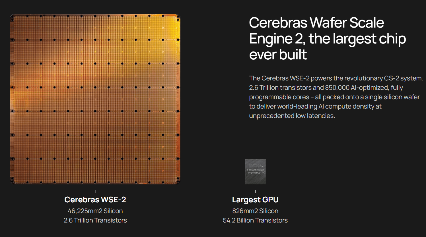
By designing the wafer as one integrated logic unit, data transfer between elements is minimized. This provides lower latency and power consumption than discrete system-on-chip or chiplet designs. While chiplets can offer flexibility by mixing and matching components, communication between chiplets is challenging. The monolithic nature of wafer-scale integration eliminates these inter-chip communication bottlenecks.
However, the ultra-large-scale also poses difficulties for manufacturability and yield with wafer-scale designs. Defects in any region of the wafer can make (certain parts of) the chip unusable. Specialized lithography techniques are required to produce such large dies. So, wafer-scale integration pursues the maximum performance gains from integration but requires overcoming substantial fabrication challenges.
Video 10.1 provides additional context about wafer-scale AI chips.
Chiplets for AI
Chiplet design refers to a semiconductor architecture in which a single integrated circuit (IC) is constructed from multiple smaller, individual components known as chiplets. Each chiplet is a self-contained functional block, typically specialized for a specific task or functionality. These chiplets are then interconnected on a larger substrate or package to create a cohesive system. Figure 10.5 illustrates this concept. For AI hardware, chiplets enable the mixing of different types of chips optimized for tasks like matrix multiplication, data movement, analog I/O, and specialized memories. This heterogeneous integration differs greatly from wafer-scale integration, where all logic is manufactured as one monolithic chip. Companies like Intel and AMD have adopted chiplet designs for their CPUs.
Chiplets are interconnected using advanced packaging techniques like high-density substrate interposers, 2.5D/3D stacking, and wafer-level packaging. This allows combining chiplets fabricated with different process nodes, specialized memories, and various optimized AI engines.
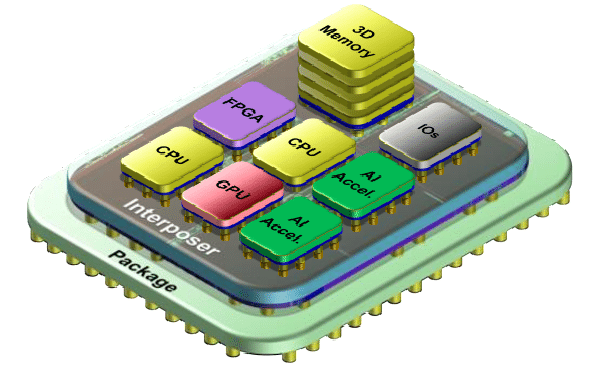
Some key advantages of using chiplets for AI include:
- Flexibility: Chiplets allow for the combination of different chip types, process nodes, and memories tailored for each function. This is more modular versus a fixed wafer-scale design.
- Yield: Smaller chiplets have a higher yield than a gigantic wafer-scale chip. Defects are contained in individual chiplets.
- Cost: Leverages existing manufacturing capabilities versus requiring specialized new processes. Reduces costs by reusing mature fabrication.
- Compatibility: Can integrate with more conventional system architectures like PCIe and standard DDR memory interfaces.
However, chiplets also face integration and performance challenges:
- Lower density compared to wafer-scale, as chiplets are limited in size.
- Added latency when communicating between chiplets versus monolithic integration. Requires optimization for low-latency interconnect.
- Advanced packaging adds complexity versus wafer-scale integration, though this is arguable.
The key objective of chiplets is finding the right balance between modular flexibility and integration density for optimal AI performance. Chiplets aim for efficient AI acceleration while working within the constraints of conventional manufacturing techniques. Chiplets take a middle path between the extremes of wafer-scale integration and fully discrete components. This provides practical benefits but may sacrifice some computational density and efficiency versus a theoretical wafer-size system.
10.8.2 Neuromorphic Computing
Neuromorphic computing is an emerging field aiming to emulate the efficiency and robustness of biological neural systems for machine learning applications. A key difference from classical Von Neumann architectures is the merging of memory and processing in the same circuit (Schuman et al. 2022; Marković et al. 2020; Furber 2016), as illustrated in Figure 10.6. The structure of the brain inspires this integrated approach. A key advantage is the potential for orders of magnitude improvement in energy-efficient computation compared to conventional AI hardware. For example, estimates project 100x-1000x gains in energy efficiency versus current GPU-based systems for equivalent workloads.
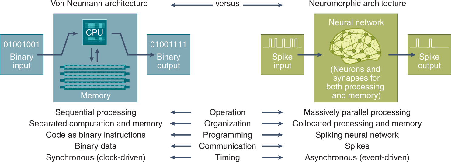
Intel and IBM are leading commercial efforts in neuromorphic hardware. Intel’s Loihi and Loihi 2 chips (Davies et al. 2018, 2021) offer programmable neuromorphic cores with on-chip learning. IBM’s Northpole (Modha et al. 2023) device comprises over 100 million magnetic tunnel junction synapses and 68 billion transistors. These specialized chips deliver benefits like low power consumption for edge inference.
Spiking neural networks (SNNs) (Maass 1997) are computational models for neuromorphic hardware. Unlike deep neural networks communicating via continuous values, SNNs use discrete spikes that are more akin to biological neurons. This allows efficient event-based computation rather than constant processing. Additionally, SNNs consider the temporal and spatial characteristics of input data. This better mimics biological neural networks, where the timing of neuronal spikes plays an important role. However, training SNNs remains challenging due to the added temporal complexity. Figure 10.7 provides an overview of the spiking methodology: (a) Diagram of a neuron; (b) Measuring an action potential propagated along the axon of a neuron. Only the action potential is detectable along the axon; (c) The neuron’s spike is approximated with a binary representation; (d) Event-Driven Processing; (e) Active Pixel Sensor and Dynamic Vision Sensor.
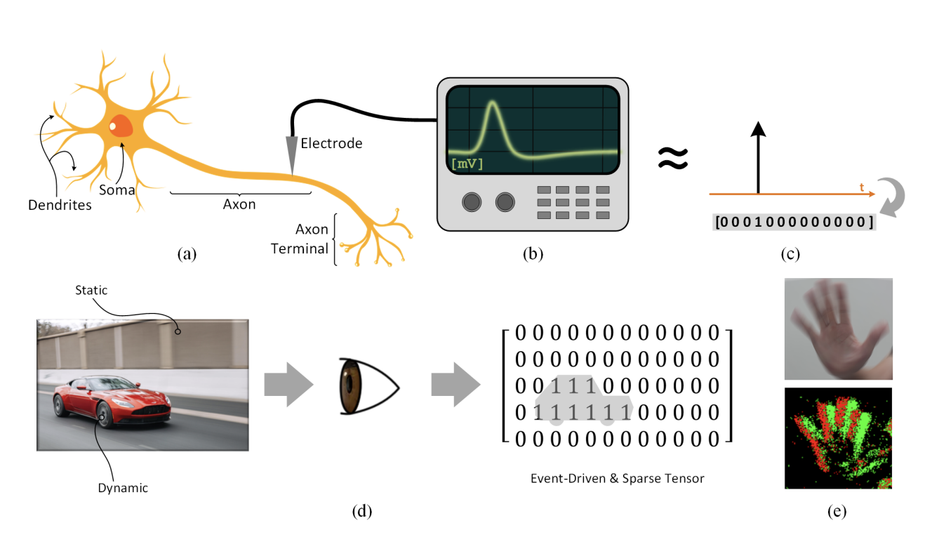
You can also watch Video 10.2 linked below for a more detailed explanation.
Specialized nanoelectronic devices called memristors (Chua 1971) are synaptic components in neuromorphic systems. Memristors act as nonvolatile memory with adjustable conductance, emulating the plasticity of real synapses. Memristors enable in-situ learning without separate data transfers by combining memory and processing functions. However, memristor technology has yet to reach maturity and scalability for commercial hardware.
The integration of photonics with neuromorphic computing (Shastri et al. 2021) has recently emerged as an active research area. Using light for computation and communication allows high speeds and reduced energy consumption. However, fully realizing photonic neuromorphic systems requires overcoming design and integration challenges.
Neuromorphic computing offers promising capabilities for efficient edge inference but faces obstacles around training algorithms, nanodevice integration, and system design. Ongoing multidisciplinary research across computer science, engineering, materials science, and physics will be key to unlocking this technology’s full potential for AI use cases.
10.8.3 Analog Computing
Analog computing is an emerging approach that uses analog signals and components like capacitors, inductors, and amplifiers rather than digital logic for computing. It represents information as continuous electrical signals instead of discrete 0s and 1s. This allows the computation to directly reflect the analog nature of real-world data, avoiding digitization errors and overhead.
Analog computing has generated renewed interest in efficient AI hardware, particularly for inference directly on low-power edge devices. Analog circuits, such as multiplication and summation at the core of neural networks, can be used with very low energy consumption. This makes analog well-suited for deploying ML models on energy-constrained end nodes. Startups like Mythic are developing analog AI accelerators.
While analog computing was popular in early computers, the boom of digital logic led to its decline. However, analog is compelling for niche applications requiring extreme efficiency (Haensch, Gokmen, and Puri 2019). It contrasts with digital neuromorphic approaches that still use digital spikes for computation. Analog may allow lower precision computation but requires expertise in analog circuit design. Tradeoffs around precision, programming complexity, and fabrication costs remain active research areas.
Neuromorphic computing, which emulates biological neural systems for efficient ML inference, can use analog circuits to implement the key components and behaviors of brains. For example, researchers have designed analog circuits to model neurons and synapses using capacitors, transistors, and operational amplifiers (Hazan and Ezra Tsur 2021). The capacitors can exhibit the spiking dynamics of biological neurons, while the amplifiers and transistors provide a weighted summation of inputs to mimic dendrites. Variable resistor technologies like memristors can realize analog synapses with spike-timing-dependent plasticity, which can strengthen or weaken connections based on spiking activity.
Startups like SynSense have developed analog neuromorphic chips containing these biomimetic components (Bains 2020). This analog approach results in low power consumption and high scalability for edge devices versus complex digital SNN implementations.
However, training analog SNNs on chips remains an open challenge. Overall, analog realization is a promising technique for delivering the efficiency, scalability, and biological plausibility envisioned with neuromorphic computing. The physics of analog components combined with neural architecture design could improve inference efficiency over conventional digital neural networks.
10.8.4 Flexible Electronics
While much of the new hardware technology in the ML workspace has been focused on optimizing and making systems more efficient, there’s a parallel trajectory aiming to adapt hardware for specific applications (Gates 2009; Musk et al. 2019; Tang et al. 2023; Tang, He, and Liu 2022; Kwon and Dong 2022). One such avenue is the development of flexible electronics for AI use cases.
Flexible electronics refer to electronic circuits and devices fabricated on flexible plastic or polymer substrates rather than rigid silicon. Unlike conventional rigid boards and chips, this allows the electronics to bend, twist, and conform to irregular shapes. Figure 10.8 shows an example of a flexible device prototype that wirelessly measures body temperature, which can be seamlessly integrated into clothing or skin patches. The flexibility and bendability of emerging electronic materials allow them to be integrated into thin, lightweight form factors that are well-suited for embedded AI and TinyML applications.
Flexible AI hardware can conform to curvy surfaces and operate efficiently with microwatt power budgets. Flexibility also enables rollable or foldable form factors to minimize device footprint and weight, ideal for small, portable smart devices and wearables incorporating TinyML. Another key advantage of flexible electronics compared to conventional technologies is lower manufacturing costs and simpler fabrication processes, which could democratize access to these technologies. While silicon masks and fabrication costs typically cost millions of dollars, flexible hardware typically costs only tens of cents to manufacture (Huang et al. 2011; Biggs et al. 2021). The potential to fabricate flexible electronics directly onto plastic films using high-throughput printing and coating processes can reduce costs and improve manufacturability at scale versus rigid AI chips (Musk et al. 2019).
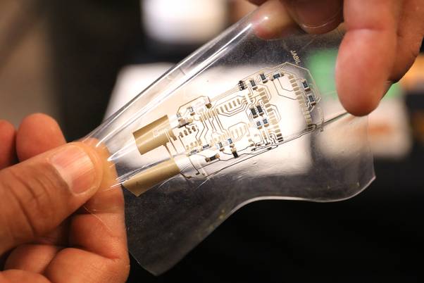
The field is enabled by advances in organic semiconductors and nanomaterials that can be deposited on thin, flexible films. However, fabrication remains challenging compared to mature silicon processes. Flexible circuits currently typically exhibit lower performance than rigid equivalents. Still, they promise to transform electronics into lightweight, bendable materials.
Flexible electronics use cases are well-suited for intimate integration with the human body. Potential medical AI applications include bio-integrated sensors, soft assistive robots, and implants that monitor or stimulate the nervous system intelligently. Specifically, flexible electrode arrays could enable higher-density, less-invasive neural interfaces compared to rigid equivalents.
Therefore, flexible electronics are ushering in a new era of wearables and body sensors, largely due to innovations in organic transistors. These components allow for more lightweight and bendable electronics, ideal for wearables, electronic skin, and body-conforming medical devices.
They are well-suited for bioelectronic devices in terms of biocompatibility, opening avenues for applications in brain and cardiac interfaces. For example, research in flexible brain-computer interfaces and soft bioelectronics for cardiac applications demonstrates the potential for wide-ranging medical applications.
Companies and research institutions are not only developing and investing great amounts of resources in flexible electrodes, as showcased in Neuralink’s work (Musk et al. 2019). Still, they are also pushing the boundaries to integrate machine learning models within the systems (Kwon and Dong 2022). These smart sensors aim for a seamless, long-lasting symbiosis with the human body.
Ethically, incorporating smart, machine-learning-driven sensors within the body raises important questions. Issues surrounding data privacy, informed consent, and the long-term societal implications of such technologies are the focus of ongoing work in neuroethics and bioethics (Segura Anaya et al. 2017; Goodyear 2017; Farah 2005; Roskies 2002). The field is progressing at a pace that necessitates parallel advancements in ethical frameworks to guide the responsible development and deployment of these technologies. While there are limitations and ethical hurdles to overcome, the prospects for flexible electronics are expansive and hold immense promise for future research and applications.
10.8.5 Memory Technologies
Memory technologies are critical to AI hardware, but conventional DDR DRAM and SRAM create bottlenecks. AI workloads require high bandwidth (>1 TB/s). Extreme scientific applications of AI require extremely low latency (<50 ns) to feed data to compute units (Duarte et al. 2022), high density (>128Gb) to store large model parameters and data sets, and excellent energy efficiency (<100 fJ/b) for embedded use (Verma et al. 2019). New memories are needed to meet these demands. Emerging options include several new technologies:
- Resistive RAM (ReRAM) can improve density with simple, passive arrays. However, challenges around variability remain (Chi et al. 2016).
- Phase change memory (PCM) exploits the unique properties of chalcogenide glass. Crystalline and amorphous phases have different resistances. Intel’s Optane DCPMM provides fast (100ns), high endurance PCM. However, challenges include limited write cycles and high reset current (Burr et al. 2016).
- 3D stacking can also boost memory density and bandwidth by vertically integrating memory layers with TSV interconnects (Loh 2008). For example, HBM provides 1024-bit wide interfaces.
New memory technologies, with their innovative cell architectures and materials, are critical to unlocking the next level of AI hardware performance and efficiency. Realizing their benefits in commercial systems remains an ongoing challenge.
In-memory computing is gaining traction as a promising avenue for optimizing machine learning and high-performance computing workloads. At its core, the technology co-locates data storage and computation to improve energy efficiency and reduce latency Wong et al. (2012). Two key technologies under this umbrella are Resistive RAM (ReRAM) and Processing-In-Memory (PIM).
ReRAM (Wong et al. 2012) and PIM (Chi et al. 2016) are the backbones for in-memory computing, storing and computing data in the same location. ReRAM focuses on issues of uniformity, endurance, retention, multi-bit operation, and scalability. On the other hand, PIM involves CPU units integrated directly into memory arrays, specialized for tasks like matrix multiplication, which are central in AI computations.
These technologies find applications in AI workloads and high-performance computing, where the synergy of storage and computation can lead to significant performance gains. The architecture is particularly useful for compute-intensive tasks common in machine learning models.
While in-memory computing technologies like ReRAM and PIM offer exciting prospects for efficiency and performance, they come with their own challenges, such as data uniformity and scalability issues in ReRAM (Imani, Rahimi, and S. Rosing 2016). Nonetheless, the field is ripe for innovation, and addressing these limitations can open new frontiers in AI and high-performance computing.
10.8.6 Optical Computing
In AI acceleration, a burgeoning area of interest lies in novel technologies that deviate from traditional paradigms. Some emerging technologies mentioned above, such as flexible electronics, in-memory computing, or even neuromorphic computing, are close to becoming a reality, given their ground-breaking innovations and applications. One of the promising and leading next-gen frontiers is optical computing technologies H. Zhou et al. (2022). Companies like [LightMatter] are pioneering the use of light photonics for calculations, thereby utilizing photons instead of electrons for data transmission and computation.
Optical computing utilizes photons and photonic devices rather than traditional electronic circuits for computing and data processing. It takes inspiration from fiber optic communication links that rely on light for fast, efficient data transfer (Shastri et al. 2021). Light can propagate with much less loss than semiconductors’ electrons, enabling inherent speed and efficiency benefits.
Some specific advantages of optical computing include:
- High throughput: Photons can transmit with bandwidths >100 Tb/s using wavelength division multiplexing.
- Low latency: Photons interact on femtosecond timescales, millions faster than silicon transistors.
- Parallelism: Multiple data signals can propagate simultaneously through the same optical medium.
- Low power: Photonic circuits utilizing waveguides and resonators can achieve complex logic and memory with only microwatts of power.
However, optical computing currently faces significant challenges:
- Lack of optical memory equivalent to electronic RAM
- Requires conversion between optical and electrical domains.
- Limited set of available optical components compared to rich electronics ecosystem.
- Immature integration methods to combine photonics with traditional CMOS chips.
- Complex programming models required to handle parallelism.
As a result, optical computing is still in the very early research stage despite its promising potential. However, technical breakthroughs could enable it to complement electronics and unlock performance gains for AI workloads. Companies like Lightmatter are pioneering early optical AI accelerators. In the long term, if key challenges are overcome, it could represent a revolutionary computing substrate.
10.8.7 Quantum Computing
Quantum computers leverage unique phenomena of quantum physics, like superposition and entanglement, to represent and process information in ways not possible classically. Instead of binary bits, the fundamental unit is the quantum bit or qubit. Unlike classical bits, which are limited to 0 or 1, qubits can exist simultaneously in a superposition of both states due to quantum effects.
Multiple qubits can also be entangled, leading to exponential information density but introducing probabilistic results. Superposition enables parallel computation on all possible states, while entanglement allows nonlocal correlations between qubits.
Quantum algorithms carefully manipulate these inherently quantum mechanical effects to solve problems like optimization or search more efficiently than their classical counterparts in theory.
- Faster training of deep neural networks by exploiting quantum parallelism for linear algebra operations.
- Efficient quantum ML algorithms make use of the unique capabilities of qubits.
- Quantum neural networks with inherent quantum effects baked into the model architecture.
- Quantum optimizers leveraging quantum annealing or adiabatic algorithms for combinatorial optimization problems.
However, quantum states are fragile and prone to errors that require error-correcting protocols. The non-intuitive nature of quantum programming also introduces challenges not present in classical computing.
- Noisy and fragile quantum bits are difficult to scale up. The largest quantum computer today has less than 1000 qubits.
- Restricted set of available quantum gates and circuits relative to classical programming.
- Lack of datasets and benchmarks to evaluate quantum ML in practical domains.
While meaningful quantum advantage for ML remains far off, active research at companies like D-Wave, Rigetti, and IonQ is advancing quantum computer engineering and quantum algorithms. Major technology companies like Google, IBM, and Microsoft are actively exploring quantum computing. Google recently announced a 72-qubit quantum processor called Bristlecone and plans to build a 49-qubit commercial quantum system. Microsoft also has an active research program in topological quantum computing and collaborates with quantum startup IonQ
Quantum techniques may first make inroads into optimization before more generalized ML adoption. Realizing quantum ML’s full potential awaits major milestones in quantum hardware development and ecosystem maturity.
10.9 Future Trends
In this chapter, the primary focus has been on designing specialized hardware optimized for machine learning workloads and algorithms. This discussion encompassed the tailored architectures of GPUs and TPUs for neural network training and inference. However, an emerging research direction is leveraging machine learning to facilitate the hardware design process itself.
The hardware design process involves many complex stages, including specification, high-level modeling, simulation, synthesis, verification, prototyping, and fabrication. Much of this process traditionally requires extensive human expertise, effort, and time. However, recent advances in machine learning are enabling parts of the hardware design workflow to be automated and enhanced using ML techniques.
Some examples of how ML is transforming hardware design include:
- Automated circuit synthesis using reinforcement learning: Rather than hand-crafting transistor-level designs, ML agents such as reinforcement learning can learn to connect logic gates and generate circuit layouts automatically. This can accelerate the time-consuming synthesis process.
- ML-based hardware simulation and emulation: Deep neural network models can be trained to predict how a hardware design will perform under different conditions. For instance, deep learning models can be trained to predict cycle counts for given workloads. This allows faster and more accurate simulation than traditional RTL simulations.
- Automated chip floorplanning using ML algorithms: Chip floorplanning involves optimally placing different components on a die. Evolutionary algorithms like genetic algorithms and other ML algorithms like reinforcement learning are used to explore floorplan options. This can significantly improve manual floorplanning placements in terms of faster turnaround time and quality of placements.
- ML-driven architecture optimization: Novel hardware architectures, like those for efficient ML accelerators, can be automatically generated and optimized by searching the architectural design space. Machine learning algorithms can effectively search large architectural design spaces.
Applying ML to hardware design automation holds enormous promise to make the process faster, cheaper, and more efficient. It opens up design possibilities that would require more than manual design. The use of ML in hardware design is an area of active research and early deployment, and we will study the techniques involved and their transformative potential.
10.9.1 ML for Hardware Design Automation
A major opportunity for machine learning in hardware design is automating parts of the complex and tedious design workflow. Hardware design automation (HDA) broadly refers to using ML techniques like reinforcement learning, genetic algorithms, and neural networks to automate tasks like synthesis, verification, floorplanning, and more. Here are a few examples of where ML for HDA shows real promise:
- Automated circuit synthesis: Circuit synthesis involves converting a high-level description of desired logic into an optimized gate-level netlist implementation. This complex process has many design considerations and tradeoffs. ML agents can be trained through reinforcement learning G. Zhou and Anderson (2023) to explore the design space and automatically output optimized syntheses. Startups like Symbiotic EDA are bringing this technology to market.
- Automated chip floorplanning: Floorplanning refers to strategically placing different components on a chip die area. Search algorithms like genetic algorithms (Valenzuela and Wang 2000) and reinforcement learning (Mirhoseini et al. (2021), Agnesina et al. (2023)) can be used to automate floorplan optimization to minimize wire length, power consumption, and other objectives. These automated ML-assisted floor planners are extremely valuable as chip complexity increases.
- ML hardware simulators: Training deep neural network models to predict how hardware designs will perform as simulators can accelerate the simulation process by over 100x compared to traditional architectural and RTL simulations.
- Automated code translation: Converting hardware description languages like Verilog to optimized RTL implementations is critical but time-consuming. ML models can be trained to act as translator agents and automate this process.
The benefits of HDA using ML are reduced design time, superior optimizations, and exploration of design spaces too complex for manual approaches. This can accelerate hardware development and lead to better designs.
Challenges include limits of ML generalization, the black-box nature of some techniques, and accuracy tradeoffs. However, research is rapidly advancing to address these issues and make HDA ML solutions robust and reliable for production use. HDA provides a major avenue for ML to transform hardware design.
10.9.2 ML-Based Hardware Simulation and Verification
Simulating and verifying hardware designs is critical before manufacturing to ensure the design behaves as intended. Traditional approaches like register-transfer level (RTL) simulation are complex and time-consuming. ML introduces new opportunities to improve hardware simulation and verification. Some examples include:
- Surrogate modeling for simulation: Highly accurate surrogate models of a design can be built using neural networks. These models predict outputs from inputs much faster than RTL simulation, enabling fast design space exploration. Companies like Ansys use this technique.
- ML simulators: Large neural network models can be trained on RTL simulations to learn to mimic the functionality of a hardware design. Once trained, the NN model can be a highly efficient simulator for regression testing and other tasks. Graphcore has demonstrated over 100x speedup with this approach.
- Formal verification using ML: Formal verification mathematically proves properties about a design. ML techniques can help generate verification properties and learn to solve the complex formal proofs needed, automating parts of this challenging process. Startups like Cortical.io are bringing formal ML verification solutions to the market.
- Bug detection: ML models can be trained to process hardware designs and identify potential issues. This assists human designers in inspecting complex designs and finding bugs. Facebook has shown bug detection models for their server hardware.
The key benefits of applying ML to simulation and verification are faster design validation turnaround times, more rigorous testing, and reduced human effort. Challenges include verifying ML model correctness and handling corner cases. ML promises to accelerate testing workflows significantly.
10.9.3 ML for Efficient Hardware Architectures
A key goal is designing hardware architectures optimized for performance, power, and efficiency. ML introduces new techniques to automate and improve architecture design space exploration for general-purpose and specialized hardware like ML accelerators. Some promising examples include:
- Architecture search for hardware: Search techniques like evolutionary algorithms (Kao and Krishna 2020), Bayesian optimization (Reagen et al. (2017), Bhardwaj et al. (2020)), reinforcement learning (Kao, Jeong, and Krishna (2020), Krishnan et al. (2022)) can automatically generate novel hardware architectures by mutating and mixing design attributes like cache size, number of parallel units, memory bandwidth, and so on. This allows for efficient navigation of large design spaces.
- Predictive modeling for optimization: ML models can be trained to predict hardware performance, power, and efficiency metrics for a given architecture. These become “surrogate models” (Krishnan et al. 2023) for fast optimization and space exploration by substituting lengthy simulations.
- Specialized accelerator optimization: For specialized chips like tensor processing units for AI, automated architecture search techniques based on ML algorithms (D. Zhang et al. 2022) show promise for finding fast, efficient designs.
The benefits of using ML include superior design space exploration, automated optimization, and reduced manual effort. Challenges include long training times for some techniques and local optima limitations. However, ML for hardware architecture holds great potential for unlocking performance and efficiency gains.
10.9.4 ML to Optimize Manufacturing and Reduce Defects
Once a hardware design is complete, it moves to manufacturing. However, variability and defects during manufacturing can impact yields and quality. ML techniques are now being applied to improve fabrication processes and reduce defects. Some examples include:
- Predictive maintenance: ML models can analyze equipment sensor data over time and identify signals that predict maintenance needs before failure. This enables proactive upkeep, which can be very handy in the costly fabrication process.
- Process optimization: Supervised learning models can be trained on process data to identify factors that lead to low yields. The models can then optimize parameters to improve yields, throughput, or consistency.
- Yield prediction: By analyzing test data from fabricated designs using techniques like regression trees, ML models can predict yields early in production, allowing process adjustments.
- Defect detection: Computer vision ML techniques can be applied to images of designs to identify defects invisible to the human eye. This enables precision quality control and root cause analysis.
- Proactive failure analysis: ML models can help predict, diagnose, and prevent issues that lead to downstream defects and failures by analyzing structured and unstructured process data.
Applying ML to manufacturing enables process optimization, real-time quality control, predictive maintenance, and higher yields. Challenges include managing complex manufacturing data and variations. But ML is poised to transform semiconductor manufacturing.
10.9.5 Toward Foundation Models for Hardware Design
As we have seen, machine learning is opening up new possibilities across the hardware design workflow, from specification to manufacturing. However, current ML techniques are still narrow in scope and require extensive domain-specific engineering. The long-term vision is the development of general artificial intelligence systems that can be applied with versatility across hardware design tasks.
To fully realize this vision, investment, and research are needed to develop foundation models for hardware design. These are unified, general-purpose ML models and architectures that can learn complex hardware design skills with the right training data and objectives.
Realizing foundation models for end-to-end hardware design will require the following:
- Accumulate large, high-quality, labeled datasets across hardware design stages to train foundation models.
- Advances in multi-modal, multi-task ML techniques to handle the diversity of hardware design data and tasks.
- Interfaces and abstraction layers to connect foundation models to existing design flows and tools.
- Development of simulation environments and benchmarks to train and test foundation models on hardware design capabilities.
- Methods to explain and interpret ML models’ design decisions and optimizations for trust and verification.
- Compilation techniques to optimize foundation models for efficient deployment across hardware platforms.
While significant research remains, foundation models represent the most transformative long-term goal for imbuing AI into the hardware design process. Democratizing hardware design via versatile, automated ML systems promises to unlock a new era of optimized, efficient, and innovative chip design. The journey ahead is filled with open challenges and opportunities.
If you are interested in ML-aided computer architecture design (Krishnan et al. 2023), we encourage you to read Architecture 2.0.
Alternatively, you can watch Video 10.3 for more details.
10.10 Conclusion
Specialized hardware acceleration has become indispensable for enabling performant and efficient artificial intelligence applications as models and datasets explode in complexity. This chapter examined the limitations of general-purpose processors like CPUs for AI workloads. Their lack of parallelism and computational throughput cannot train or run state-of-the-art deep neural networks quickly. These motivations have driven innovations in customized accelerators.
We surveyed GPUs, TPUs, FPGAs, and ASICs specifically designed for the math-intensive operations inherent to neural networks. By covering this spectrum of options, we aimed to provide a framework for reasoning through accelerator selection based on constraints around flexibility, performance, power, cost, and other factors.
We also explored the role of software in actively enabling and optimizing AI acceleration. This spans programming abstractions, frameworks, compilers, and simulators. We discussed hardware-software co-design as a proactive methodology for building more holistic AI systems by closely integrating algorithm innovation and hardware advances.
But there is so much more to come! Exciting frontiers like analog computing, optical neural networks, and quantum machine learning represent active research directions that could unlock orders of magnitude improvements in efficiency, speed, and scale compared to present paradigms.
Ultimately, specialized hardware acceleration remains indispensable for unlocking the performance and efficiency necessary to fulfill the promise of artificial intelligence from cloud to edge. We hope this chapter provides useful background and insights into the rapid innovation occurring in this domain.
10.11 Resources
Here is a curated list of resources to support students and instructors in their learning and teaching journeys. We are continuously working on expanding this collection and will add new exercises soon.
- Coming soon.
- Coming soon.